High-Voltage Motor Driver with Safety Interlocks
Overview
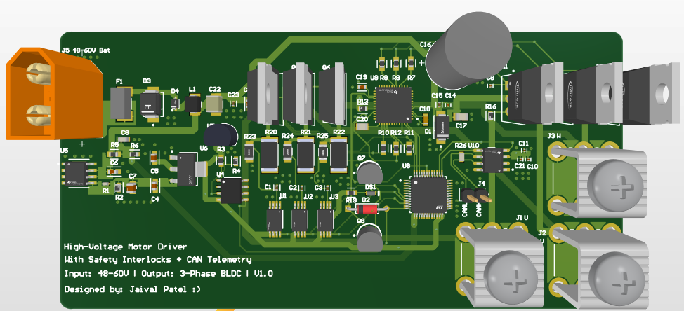
The High-Voltage Motor Driver with Safety Interlocks is a 4-layer, high-current PCB designed for driving BLDC motors in safety-critical environments. Featuring a DRV8353 gate driver, N-channel MOSFET half-bridge, diode-OR hardware shutdown logic, and STM32 control with CAN interface, this design is optimized for robustness, isolation, and system-wide interlock integration.
Key Features
This section details the major electrical and architectural decisions, component justifications, and circuit integration strategies employed in this project.
Gate Driver – DRV8353RSRGZT
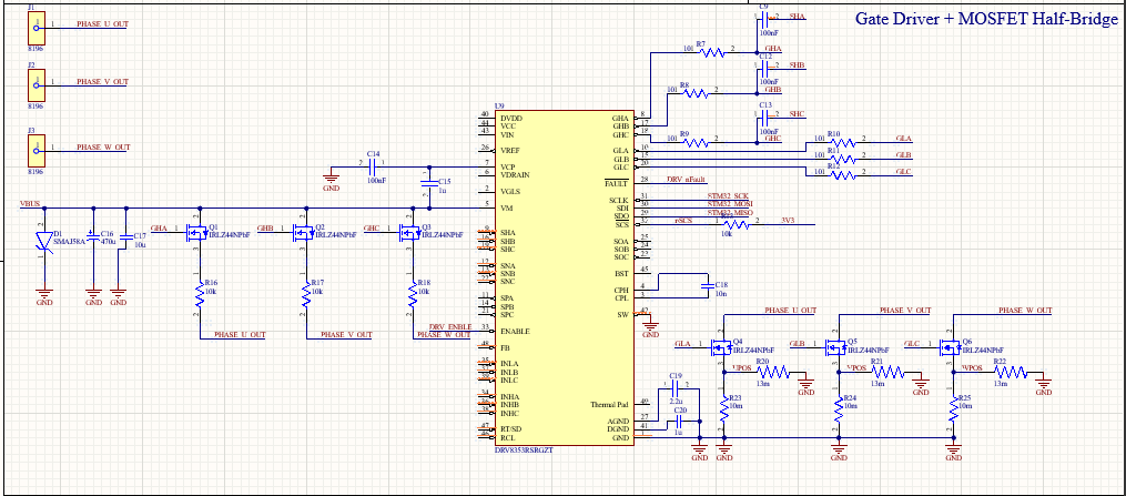
The DRV8353 was chosen for its high-performance 3-phase gate driving capabilities, integrated current shunt amplifiers, SPI configurability, and fault reporting. Among alternatives like the DRV8305 and discrete gate drivers (e.g., IR2110), the DRV8353 offered the most flexibility with its SPI diagnostics and protection features. I chose the RSRGZT package for space efficiency and thermal performance.
2. Power Stage – Half-Bridge MOSFETs
I used IRLZ44NPBF N-channel MOSFETs due to their low Rds(on), fast switching, and robust thermal handling at moderate cost. Their TO-220 footprint was ideal for symmetrical layout and heat sinking. Symmetrical placement minimized inductive parasitics, and gate resistors were used for slew rate control. View Figure 2 for more details.
3. ENABLE Interlock – Fault Logic
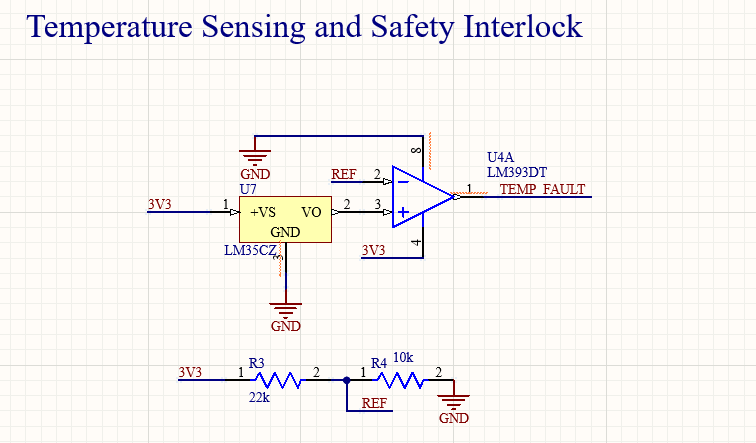
A diode-OR logic circuit (TEMP_FAULT, DRV_nFAULT, MCU_SHUTDOWN) feeds into a 2N3904 NPN transistor, which pulls ENABLE low to shut off the DRV8353. This hardware-based override ensures immediate response during a thermal or driver failure. The 1N4148 diodes were selected for their speed and low forward drop.
Debug & Telemetry – CAN Interface
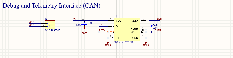
Instead of UART, I adopted CAN using the SN65HVD230 transceiver with RS grounded to enable high-speed mode. CAN is more robust in noisy environments, allows multi-node diagnostics, and better matches automotive and industrial standards. I mapped CANH/CANL to STM32's Tx/Rx through the transceiver's D and R pins.
STM32 Microcontroller
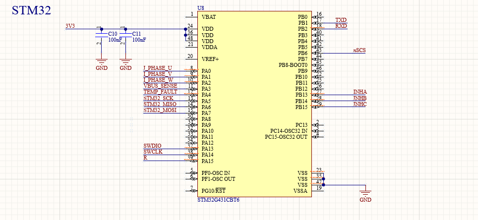
The STM32F103C8T6 was selected for its affordability, abundant documentation, support for CAN peripherals, and STM32Cube ecosystem. Its GPIO and interrupt capabilities were critical for real-time fault response. I leveraged its ADC to monitor analog parameters and its NVIC for handling nFAULT, TEMP_FAULT, and comms asynchronously.
Voltage Regulation
The AMS1117-3.3 linear regulator was used to supply 3.3V to the STM32 and logic circuitry. Despite being a linear regulator, it offered sufficient performance due to low current draw and simplicity. Power dissipation was calculated under worst-case scenarios to ensure thermal margins were met.
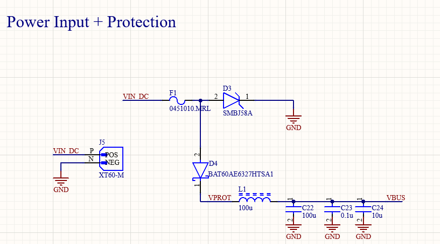
Power Input – XT60 Connector
The AMASS XT60-M connector was selected for its high-current capability (up to 60A), polarized housing, and reliable mating. It was mounted with reinforced pads and routing to handle peak loads and prevent PCB delamination. View Figure 7 for more details.
Layer Stackup
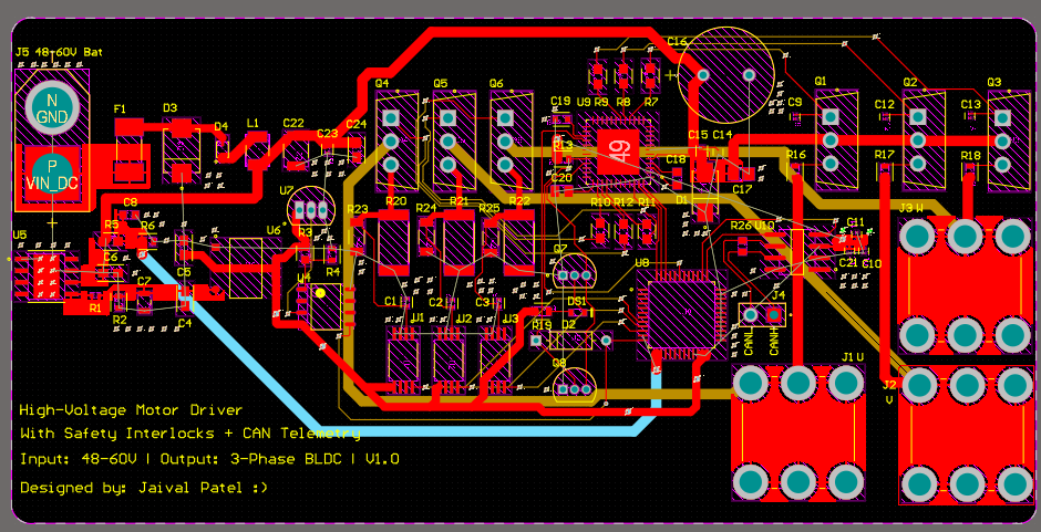
I used a 4-layer stackup: Power + Component (Top), Signal, Power (Inner), GND (Bottom). This supported:
- Improved EMI performance with bottom GND shield
- Controlled impedance routing
- Dedicated planes for motor phase and logic power
PCB Layout Strategy
The board layout was done in Altium Designer with a focus on thermal performance, signal isolation, and safety.
Symmetrical Half-Bridge Layout
The MOSFET half-bridges were laid out symmetrically with source-drain alignment and short gate traces to reduce inductive loops. GND return paths were kept tight, and shunt resistors were placed near the low-side source.
Separation of Power and Logic
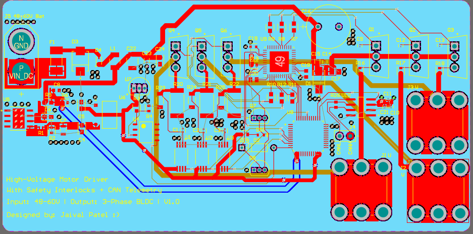
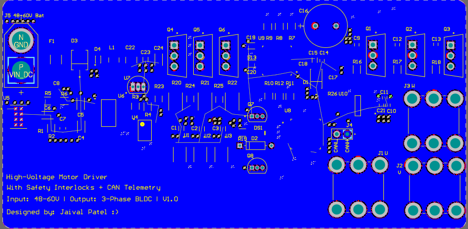
High-power and low-voltage circuits were isolated physically and electrically. Signal traces were routed away from switching nodes. The GND plane acted as a shield, with analog and digital grounds stitched near the regulator.
Fault Logic Placement
The 2N3904-based shutdown circuit was placed near the ENABLE line, with minimal trace length. All fault signal lines were pulled high with 10k resistors and bypassed with 100nF caps for noise immunity.
Decoupling Strategy
Local decoupling capacitors (10uF + 0.1uF) were placed near each IC power pin, especially the DRV8353 and STM32. Layout guidelines for power planes and return current paths were followed to minimize high-frequency noise.
CAN Trace Routing
CANH and CANL were routed as a tightly coupled differential pair with matched length, 120-ohm termination, and proper isolation from power signals. The transceiver was placed near the edge for easy connector access.
Challenges & Constraints
- Mixed-Signal Isolation: Balancing digital and analog/motor noise domains required careful stitching, ground management, and shielding strategy.
- Thermal Performance: Managing MOSFET and gate driver heat without heat sinks was constrained by footprint and airflow assumptions.
- Real-Time Fault Response: Ensuring deterministic shutdown required both hardware fallback and fast microcontroller interrupt handling.
- Component Placement: With a compact board size, routing the ENABLE fault logic and CAN without overlaps was non-trivial.
Tools Used
- Altium Designer: Schematic capture and 4-layer PCB layout
- STM32CubeIDE: Firmware development and peripheral setup
- MATLAB: (Planned) Motor performance simulation and trip threshold analysis
- Multimeter & Logic Analyzer: Validation of ENABLE logic and CAN communication
Outcome & Future Work
The board was fabricated successfully, passed power-on tests, and verified DRV8353 configuration and fault reporting via SPI. CAN messages were received over a differential bus. Future work includes:
- Integrating closed-loop control for torque and speed
- Thermal camera validation under PWM load
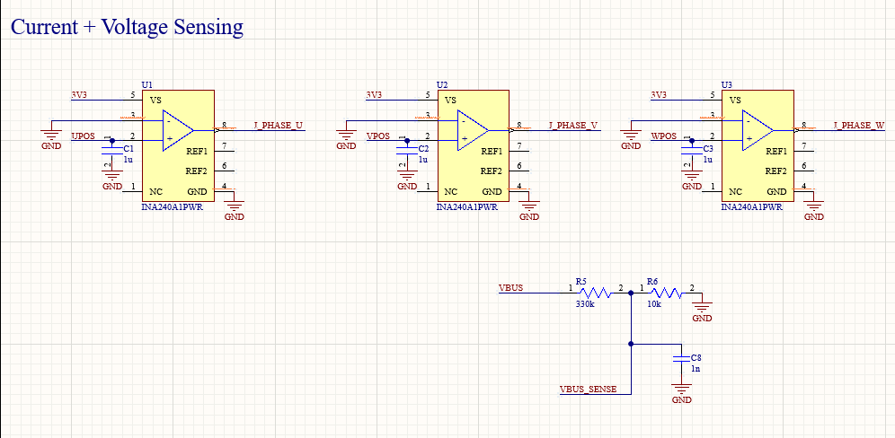
- Adding analog feedback for phase current and voltage sensing