Thermal Safety Board with Analog Front End
Overview
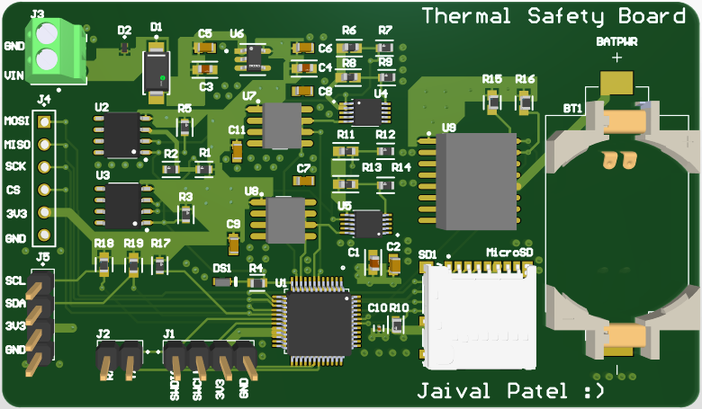
The Thermal Safety Board is a 6-layer embedded system designed to monitor temperature thresholds using analog thermistors, trigger hardware-level shutdown responses, and optionally log thermal events to microSD with real-time timestamps. It leverages a comparator-driven trip circuit, STM32F103C8T6 MCU control, and multiplexed analog front-end design to reduce part count while supporting multiple thermal sensing channels.
In high-density embedded environments, such as battery management or motor control enclosures, thermal runaway can cause irreversible system damage. Many systems rely on software polling for protection, which can be too slow or unreliable. This board adds a dedicated analog safety layer for immediate hardware override, while providing digital telemetry for analysis and prediction. Its form factor and power model target small form-factor industrial and robotics environments.
Key Features & Design Decisions
The Thermal Safety Board was developed as a failsafe response system for embedded platforms subject to heat-sensitive operation. Each hardware decision was made with minimal latency, hardware reliability, and analog accuracy in mind. This system prioritizes edge-triggered thermal monitoring through a comparator-driven logic chain, while also offering microcontroller-level telemetry and optional logging. Below, we explore the design rationale behind its core components and architecture.
Hardware Trip Logic (LM393)
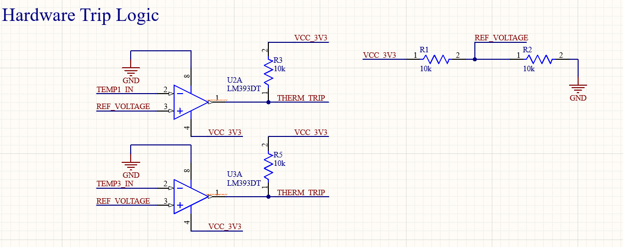
At the heart of the safety function lies the LM393 dual comparator, chosen for its open-drain output and low quiescent current. Its job is to compare the voltage generated from a thermistor-based divider against a known reference voltage (REF_VOLTAGE) and trigger a THERM_TRIP line when thresholds are exceeded. Unlike software polling or ADC interrupt solutions, the LM393 reacts in microseconds, offering true hardware-layer protection. It also supports hysteresis through positive feedback to prevent output chatter due to noise near threshold crossings.
The dual comparator was selected over quad variants for board area and simplicity, as only one channel is actively monitored for triggering the system trip line. The open-drain design was critical in allowing multiple comparators to share a THERM_TRIP line without electrical conflict in future multi-zone expansions.
STM32F103C8T6 Microcontroller
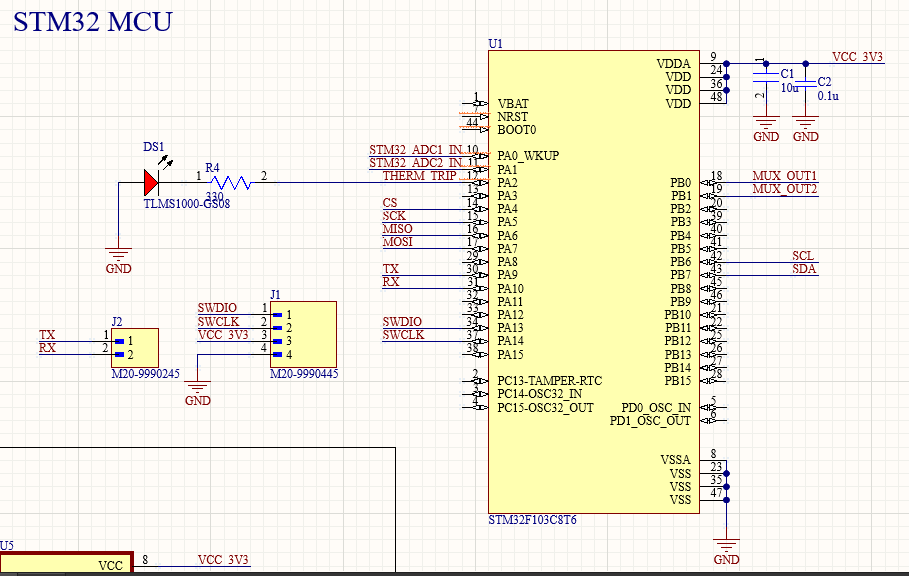
The STM32F103C8T6 was selected due to its:
- 12-bit ADC for precision voltage readouts from the thermistor divider
- Multiple UART channels for logging and debugging
- Low power consumption compatible with battery-based thermal boards
- Bootloader support for firmware updates without extra components
This device provides the backbone for periodic temperature telemetry, status LED control, and serial interface feedback. The ADC periodically samples each channel using a polling loop and integrates hysteresis flags for software redundancy.
microSD + RTC Logging Support
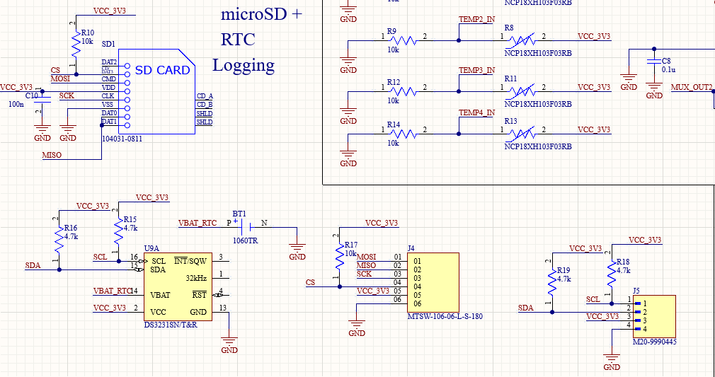
Although not populated in the initial prototype, the board includes pads for a microSD breakout and DS3231 RTC module. The intention is to allow logging of time-stamped overtemperature events and temperature profiles. This is particularly useful in debugging faults from high-power battery packs or power electronics where retroactive thermal review is critical.
The microSD follows the same SPI-based design used in previous projects: level-shifted SPI with CS controlled from the STM32, and an RC-filtered 3.3V power rail. The DS3231 RTC communicates over I2C with its own pull-ups and an integrated crystal oscillator, minimizing component count and drift.
Power Supply: CR2032 Cell
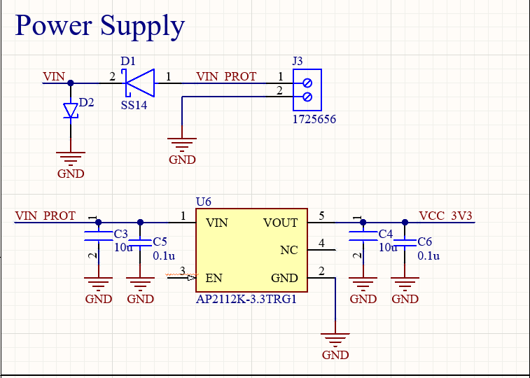
The board is powered by a CR2032 coin cell, regulated through an LDO for consistent 3.3V operation. This power topology was selected for its low power consumption, isolation from host systems, and long shelf life. The analog chain and STM32 operate within a 1–5 mA range under active sensing, allowing 50–100 hours of intermittent use.
The analog portion is isolated via decoupling capacitors near the op-amp and thermistor dividers, and the comparator supply is filtered to ensure the REF_VOLTAGE stability under sudden loads.
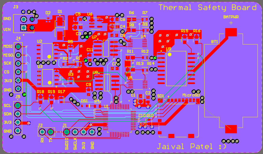
PCB Layout Strategy
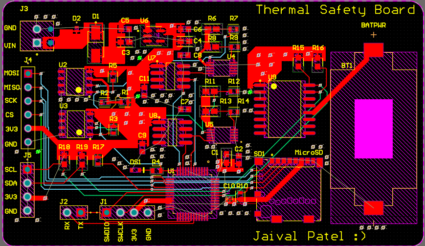
The Thermal Safety Board was designed using a 6-layer stackup to manage thermal sensitivity, analog-digital signal integrity, and low-noise comparator response. This decision ensured enough routing space to separate digital UART and STM32 lines from analog multiplexers and trip logic, while maintaining predictable return paths and reference planes.
Layer Stackup Overview
- Top (L1): Power + Components
- Layer 2: Power
- Layer 3: Signal
- Layer 4: Signal
- Layer 5: VCC_3V3 Power
- Bottom (L6): GND
Thermal Trip Logic Placement
The LM393 comparator and REF_VOLTAGE divider were placed in the lower-left analog region of the board, near the thermistor header. This minimized trace length from the divider node to the comparator input and allowed short, wide routing from the reference voltage divider.
The REF_VOLTAGE divider was routed with a wide trace from the regulated 3.3V plane on Layer 3 and included a bypass capacitor located <2mm from the comparator Vcc. The output THERM_TRIP line was routed with a single via to the STM32 pin, with strong pull-up via a 10kΩ resistor to reduce false triggering.
STM32 Routing
The STM32F103 was centrally placed, surrounded by:
- UART header on the top-right edge for access to TX/RX
- SWD debugging header placed orthogonally to avoid conflict with power rails
- Analog ADC inputs for the thermistor chain on the bottom-left GPIO bank
Analog MUX Isolation
The two TS5A23159 muxes were placed in the upper-left corner, separated from STM32 and UART lines by a ground moat and copper pour boundary. Each MUX was connected to a distinct thermistor pair and routed through to the op-amp via short, guarded traces. Select lines were driven by STM32 GPIOs routed on Layer 4, with edge-clearance spacing to avoid overlap with the thermal plane.
Grounding Strategy
Layer 2 served as the primary ground plane, with no breaks under analog signal paths. All vias from decoupling capacitors were stitched directly to this layer, ensuring <100mΩ impedance from every return path. LM393 and MCP602 components were mounted with ground reliefs to ensure their thermal islands tied uniformly to the copper pour.
Power and Filtering
The CR2032 input feeds into a reverse polarity diode and RC filter before entering the 3.3V rail. From there, power is distributed along Layer 3 to:
- STM32
- Comparator + REF_VOLTAGE divider
- LED indicator logic
- Analog muxes
Header Access and Silkscreen
All external access points (UART, SWD, sensor input) are labeled with function and voltage domain. Test points are exposed on the right side of the board for 3.3V, THERM_TRIP, and REF_VOLTAGE.
Thermal Drift Simulation in MATLAB
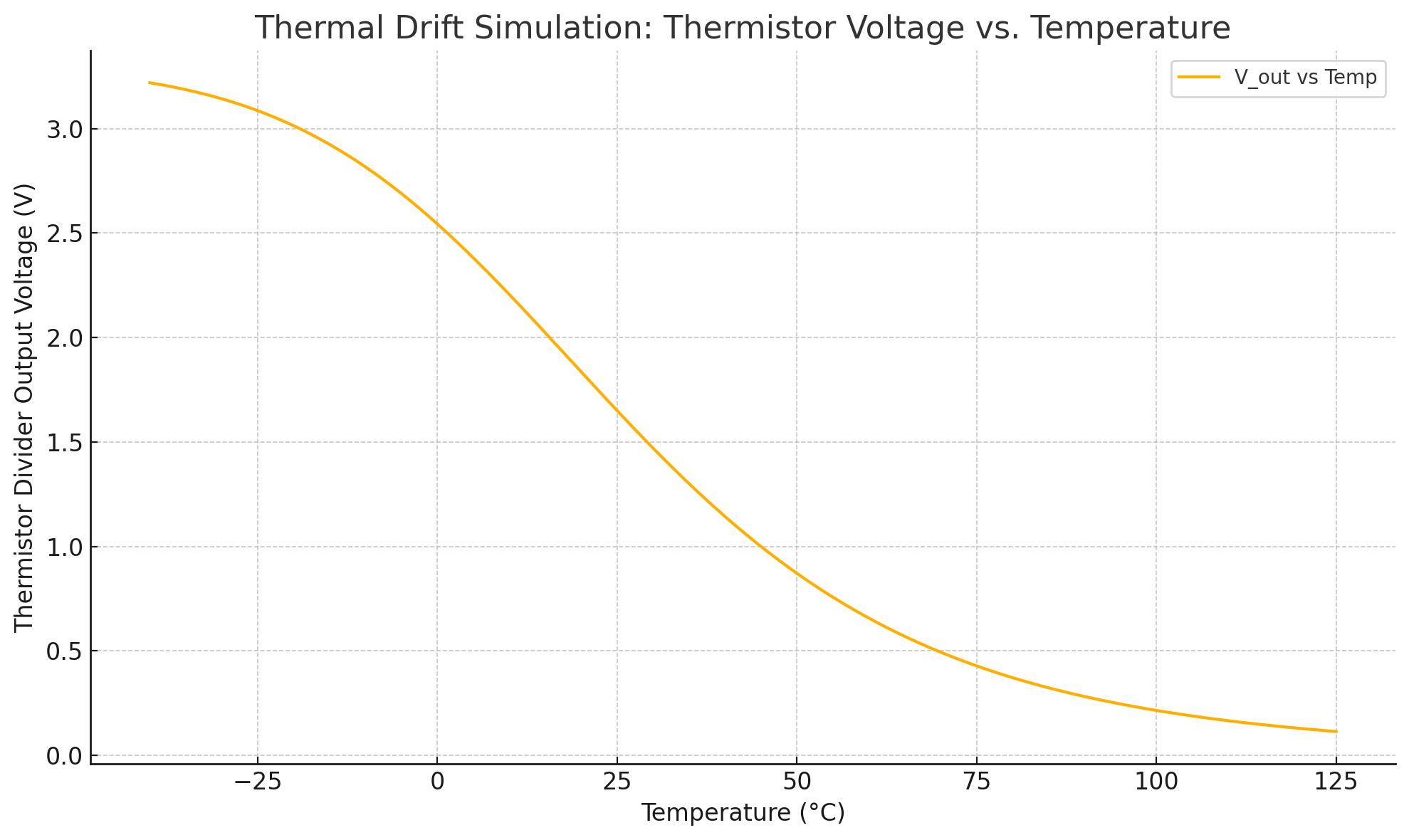
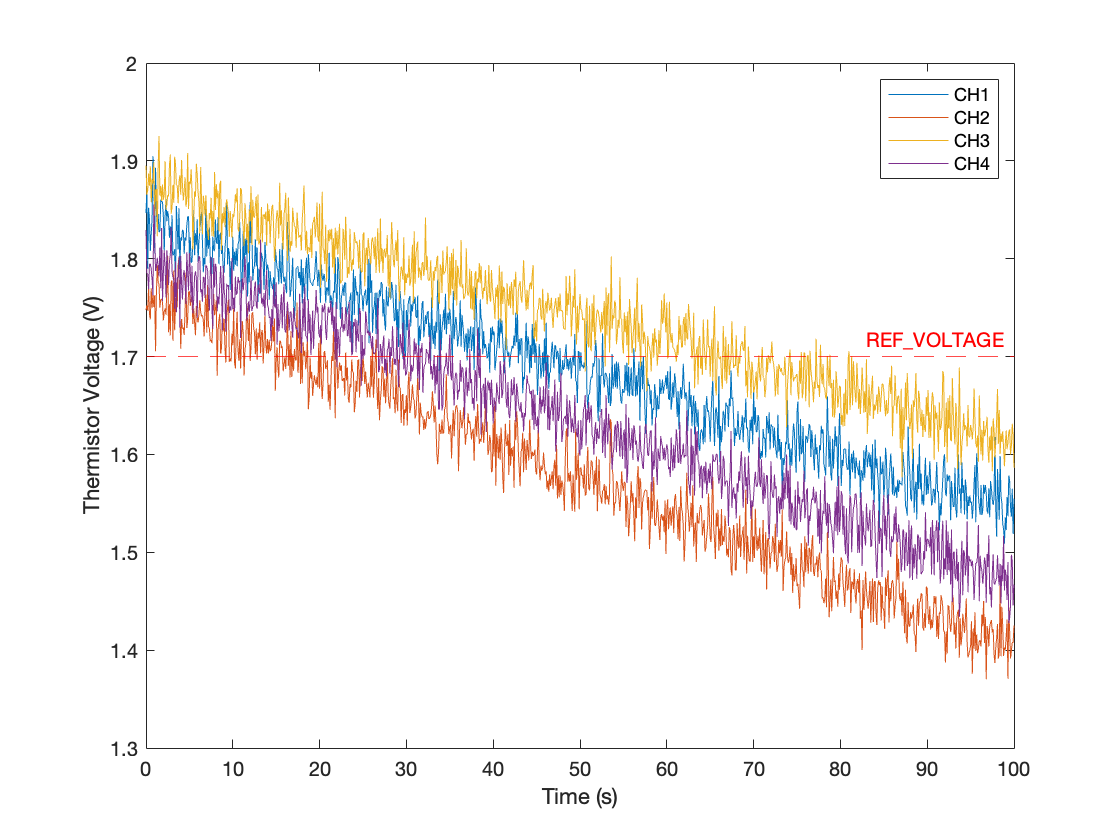
The MATLAB simulation was used to model thermistor behavior over time and validate system trip thresholds under noisy conditions. The simulation mimics gradual heating due to environmental stress and applies voltage divider logic to identify the REF_VOLTAGE crossing point.
% Thermal voltage simulation for 4 channels
time = 0:0.1:100;
T_base = [20 22 19 21]; % starting temp in Celsius
drift = [0.08 0.1 0.07 0.09]; % degree per second
REF = 1.7; % trip threshold voltage
noise = 0.02 * randn(length(time),4);

for ch = 1:4
    temp(:,ch) = T_base(ch) + drift(ch) * time;
    R = 10000 * exp(3950*(1./(temp(:,ch)+273.15)-1/298.15));
    Vout(:,ch) = (R ./ (R + 10000)) * 3.3 + noise(:,ch);
end

plot(time, Vout); yline(REF, 'r--', 'REF\_VOLTAGE');
xlabel('Time (s)'); ylabel('Thermistor Voltage (V)');
legend('CH1','CH2','CH3','CH4');
The simulation shows each thermistor voltage response increasing non-linearly as the temperature rises. As expected, voltage across the fixed divider increases as thermistor resistance drops. Channel 2 reaches the REF_VOLTAGE threshold earliest due to a slightly faster drift rate. This illustrates the system's ability to discriminate between small thermal gradients and respond accordingly.
The red dashed line represents the analog trip threshold set in hardware. As each channel's voltage crosses this line, the LM393 comparator triggers the THERM_TRIP signal. The presence of superimposed noise validates that the trip signal remains stable even with ±20mV analog variation.
This analysis confirms that the REF_VOLTAGE threshold is well-tuned to catch slow-rising thermal faults with minimal false positives. It also supports hysteresis tuning by revealing how margin is affected by slope rate and noise. These results validate both the hardware comparator performance and the ADC sampling code implemented on the STM32.
Challenges & Debugging
- Comparator oscillation solved by tuning hysteresis feedback
- Multiplexer leakage resolved by sourcing TS5A23159 with matched Ron range
- Thermistor polarity flipped during early bring-up; resolved with resistor mirror
- UART TX line clashed with LED array logic — pin remapping applied
Tools & Skills Used
- Altium – Full schematic and 6-layer layout
- STM32CubeIDE – ADC polling, UART debug, comparator flags
- MATLAB – Thermal model simulation and validation
- Logic analyzer – Analog mux validation
Future Work
- Add buck converter and input protection for higher-current safety applications
- Incorporate supervised watchdog logic for STM32 timeout fallback
- Expand to 8-channel sensing with overtemperature filtering