Tesla Infotainment System
Overview
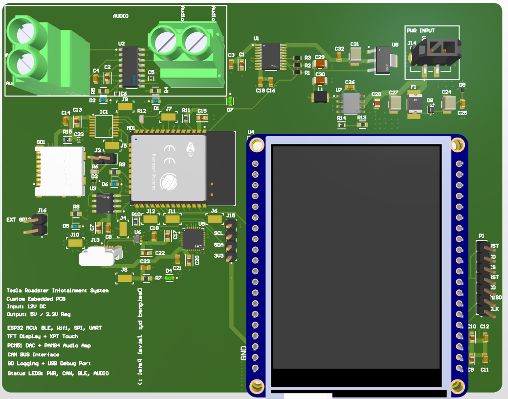
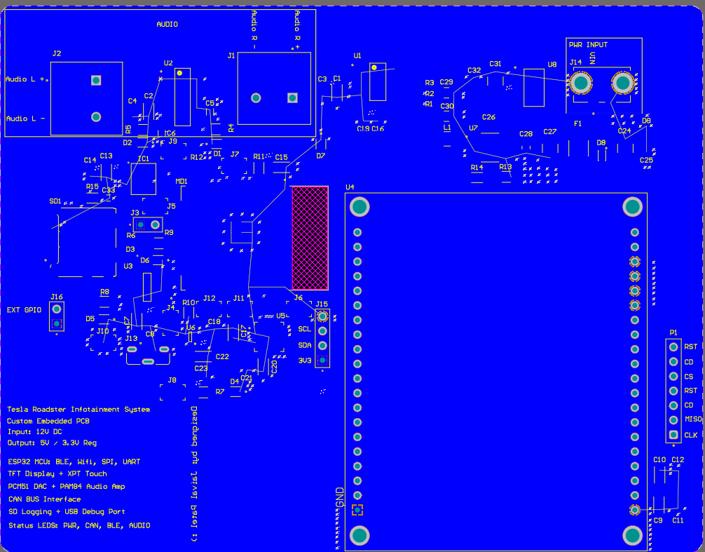
The Tesla Roadster Infotainment System project is a custom-engineered 8-layer embedded PCB designed to deliver a robust, responsive, and feature-rich in-vehicle infotainment interface. Inspired by—but distinctly improved from—an open-source Tesla infotainment module, this board was architected from scratch to address noise isolation, signal routing efficiency, layout compactness, and audio-visual integration challenges often overlooked in open designs.
While the open-source reference board served as an architectural baseline, our design restructured the stackup, re-routed power domains for greater thermal stability, and redesigned the human-machine interface (HMI) circuitry for enhanced responsiveness. Notably, the capacitive touch and TFT display interfaces were isolated via cleaner SPI routing and decoupled voltage planes to reduce cross-domain EMI and improve visual clarity during runtime.
The system is powered by a high-efficiency MP1584EN buck converter, with proper filtering and isolation stages to minimize ripple artifacts in sensitive analog sections—an area where the original design suffered from audio distortion and ESP32 instability. A dedicated PAM8403 stereo amplifier was integrated to drive onboard audio output with sufficient fidelity and volume, avoiding the coupling noise issues present in the earlier community design.
Core functions are driven by an ESP32-WROOM module that manages BLE/Wi-Fi, ILI9341 TFT display updates, XPT2046 capacitive touch inputs, and button matrix events in real-time. A CAN transceiver (SN65HVD230) enables future expansion for vehicle integration. USB-C support provides both power and serial development access, and all subsystems were rerouted to improve electrical partitioning and reduce layout congestion.
Altogether, the redesign presents a refined, more scalable infotainment system suitable for custom EV builds or as a testbed for next-generation cabin UX experiments—highlighting system-level design thinking, layout optimization, and real-world interface tuning.
Key Features
1. MP1584EN Buck Regulator – Power Distribution Backbone
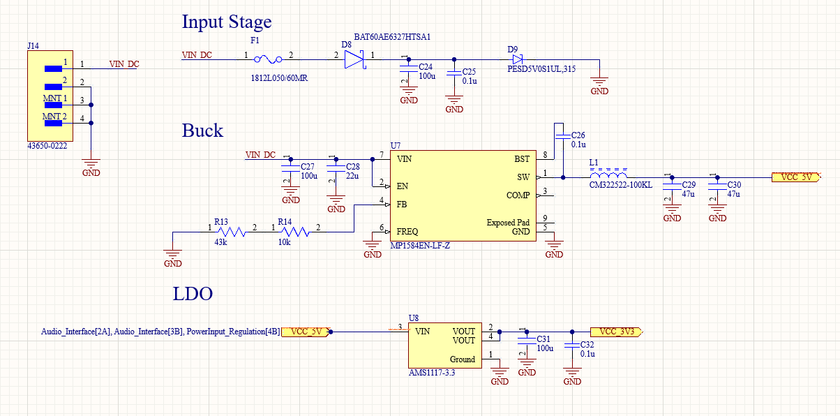
The MP1584EN was selected as the primary power supply IC to step down 12V automotive input to a stable 5V rail. It supports up to 3A output current, ideal for powering ESP32, TFT display, audio amplifier, and touch IC simultaneously. Key reasons for its selection include:
- Wide input range (4.5V to 28V) for automotive compatibility
- High efficiency (~90%) with minimal thermal rise
- Fixed-frequency operation for predictable EMI behavior
We added external 22μH inductor and low-ESR ceramic capacitors for output filtering. The COMP and FREQ pins were left floating, using internal defaults for ease of layout and minimizing external noise sensitivity.
2. ESP32-WROOM-32E – Embedded Controller with BLE + Wi-Fi
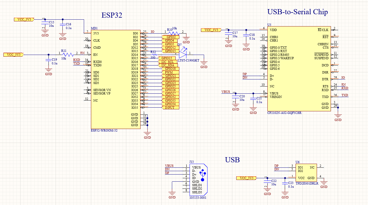
The ESP32 module handles:
- BLE communication with paired devices
- TFT screen updates via SPI
- Capacitive touch position decoding
- Debounced button matrix interface
We chose the ESP32-WROOM-32E variant for its stable silicon revision, large RAM/flash, and excellent community support. Its multi-core architecture allowed decoupling BLE tasks from display refresh loops, and SPI DMA modes were used to accelerate rendering without overloading CPU.
3. ILI9341 TFT Display + XPT2046 Touchscreen Controller
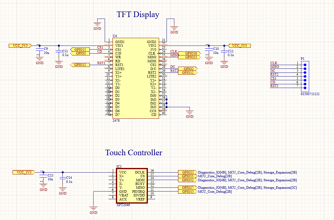
This SPI-based 320x240 TFT module was integrated for HMI display, while the XPT2046 chip provided capacitive touch tracking. We improved upon the open-source layout by:
- Separating SPI clock lines for display and touch controllers
- Using 33Ω series resistors on SPI to damp reflections
- Placing both components along one edge to ease ribbon cable routing
Additionally, we used a shared 5V→3.3V LDO (AMS1117) to power the ILI9341 and XPT2046 with decoupled bulk caps to reduce cross-device ripple coupling.
4. PAM8403 Stereo Class-D Audio Amplifier
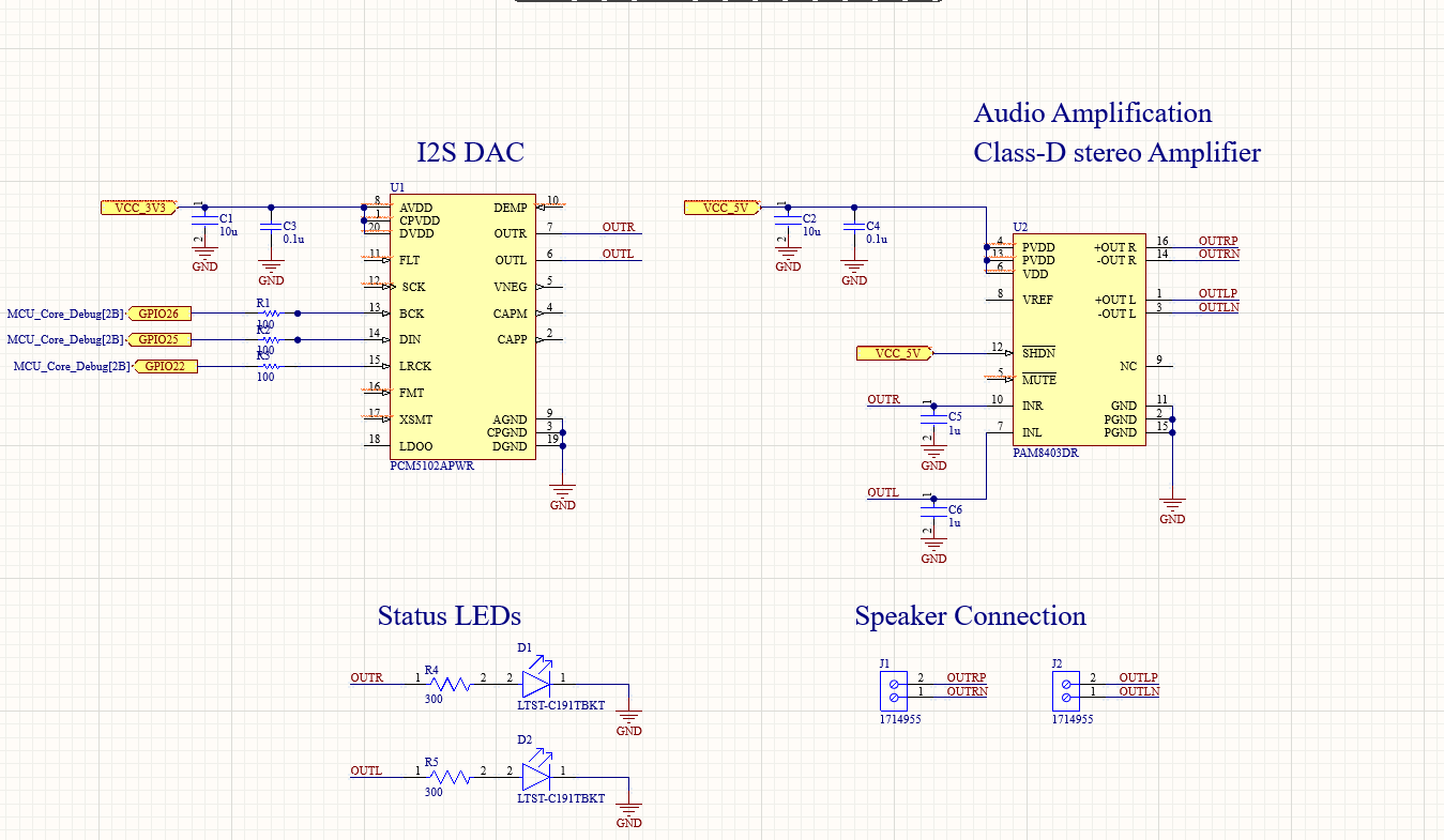
The PAM8403 was selected for its 3W/channel output, filterless operation, and 90% efficiency at 5V input. It simplified layout by eliminating external inductors. Our design:
- Placed the amplifier away from SPI traces to avoid noise injection
- Included pop-suppression RC filters at the speaker outputs
- Used large trace widths and short paths for speaker power routing
The original design suffered from speaker hum due to poor power domain isolation. We addressed this by adding a ferrite bead between MP1584EN and PAM8403 input, with local ceramic filtering.
6. USB-C Connector – Dual Role Power & Debug
As seen in Figure 3, a USB-C breakout was used to supply 5V power to the board and provide serial programming/debug interface. ESD protection diodes (PESD5V0S1UL) were added at the D+ and D− lines. The CH340C USB-UART bridge was used for minimal footprint and automatic reset wiring with ESP32's EN and IO0 lines.
7. SN65HVD230 CAN Transceiver
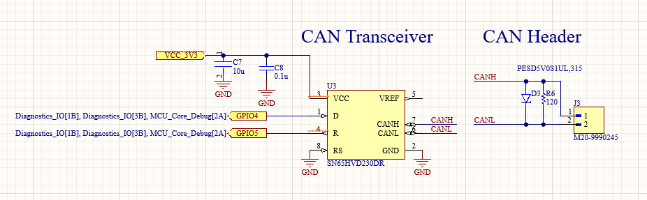
To support future expansion into full EV-CAN networks, a SN65HVD230 was integrated. The RS pin was tied low for high-speed mode. CANH and CANL lines were routed as a differential pair with 120Ω termination across header pins. While not yet utilized, this transceiver was strategically included for roadmap flexibility.
PCB Layout Strategy
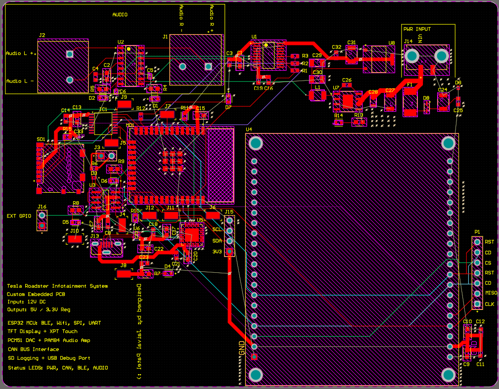
The PCB layout for the Tesla Roadster Infotainment System board was a critical aspect of the overall system design, with decisions made to optimize for signal integrity, thermal efficiency, mechanical reliability, and production scalability. This was not a simple routing task—it was an exercise in architectural partitioning, functional prioritization, and manufacturability planning, given the dense integration of multimedia, power, analog, and digital domains across an 8-layer board.
1. Layer Stackup and Global Layout Partitioning
The board was designed as an 8-layer structure with the following stackup:
- Top Layer – Power + Signal (Component Mounting Layer)
- Layer 2 – Power1 (Dedicated 3.3V polygon pours)
- Layer 3 – Power2 (Shared analog + digital power zones)
- Layer 4 – Signal1 (Primary digital communication routing)
- Layer 5 – Signal2 (Secondary signals, BLE antenna routing)
- Layer 6 – Signal3 (Auxiliary buses, backlight dimming, I²S)
- Layer 7 – Signal4 (Control signals, LED arrays)
- Bottom Layer – GND (Solid, stitched reference)
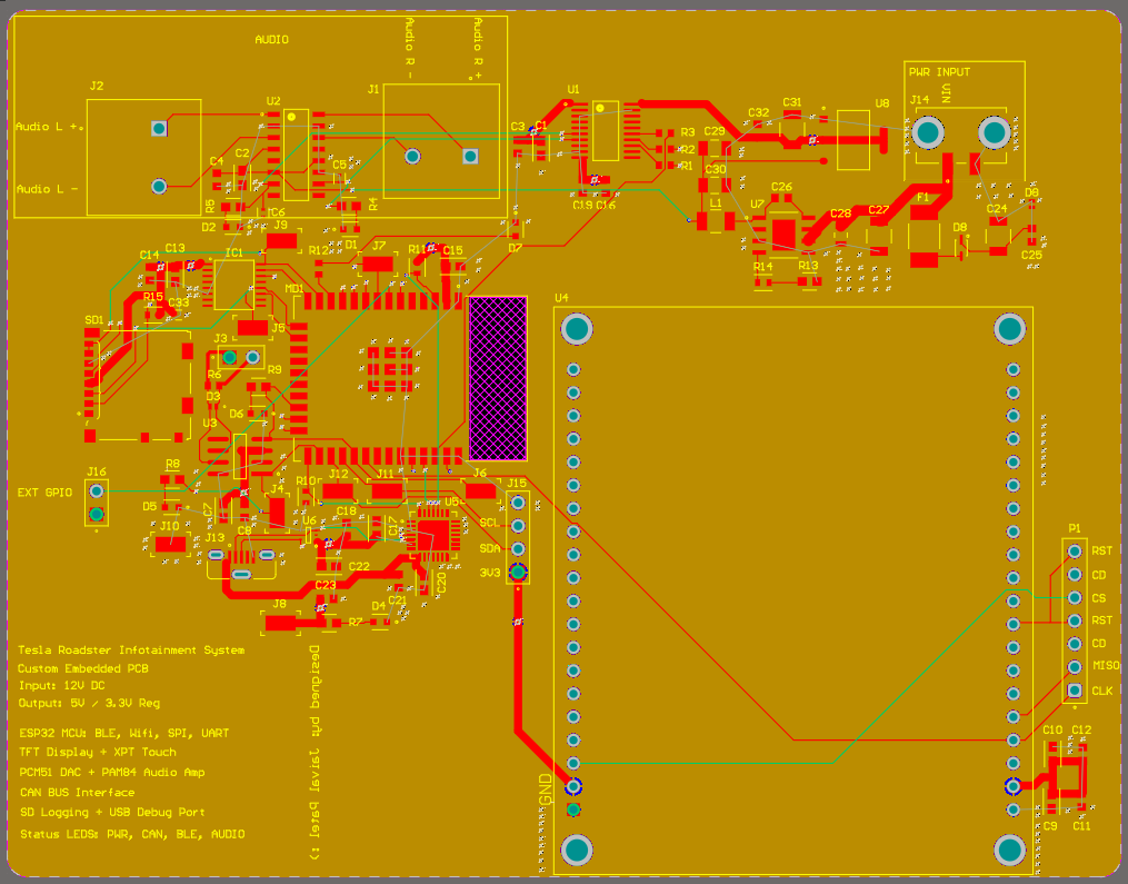
2. Functional Zoning & Placement Philosophy
Functional blocks were deliberately placed based on thermal performance, user interface accessibility, and noise segregation. For instance, the MP1584EN buck converter was top-left for thermals and input isolation; the STM32F103 and ESP32-WROOM digital core was centered; and the PAM8403 audio amp sat bottom-left with thermal vias beneath. BLE antenna clearance zones were enforced on layers 1–5.
3. Via Strategy and Inter-layer Routing
We employed through-hole vias, blind vias, and dense stitching:
- Power vias dropped from buck/LDOs into Power1/Power2
- Signal vias for SPI, I²S, UART routed through Signal1–Signal3
- Thermal vias under MP1584EN and PAM8403 aided dissipation
- Via stitching around GND borders and between reference planes reduced EMI and increased rigidity
4. Trace Width, Length, and Impedance
- SPI Lines: 10 mil wide, matched within 5%, spaced 6 mil
- I²S Audio: 15 mil with adjacent GND shielding
- Power Traces: 3.3V @ 50–70 mil; audio/backlight @ 80 mil; widths calculated using IPC-2221
5. EMI and Crosstalk Mitigation
- BLE keep-out zones cleared on multiple layers
- Guard traces and grounded pours around analog audio
- Backlight PWM routed as differential pair to minimize coupling
- Analog/digital GND islands tied at a single star point beneath LDO
6. Component Orientation and Accessibility
All connectors were edge-aligned for ease of access. Test points for SPI, UART, I²S, and reset were exposed with labeled silkscreen. All components were top-mounted for reflow compatibility.
7. Silkscreen, Annotation, and Assembly
- Text height ≥ 0.8mm for legibility
- Arrows for signal direction, polarity indicators for caps/LEDs
- QR code linked to GitHub docs
8. Lessons Learned and Optimization
- Series 22Ω resistors helped SPI bus stability
- Audio noise solved by GND plane break under MP1584EN
- BLE antenna rerouted after RSSI drop caused by pour overlap
Challenges & Constraints
Designing the Tesla Roadster Infotainment System board presented several unique technical challenges, spanning electrical, mechanical, thermal, and electromagnetic domains. Many of these constraints stemmed from adapting and improving upon an open-source reference design while enhancing it for robustness, manufacturability, and field deployment. Each design tradeoff was carefully evaluated in the context of automotive requirements for reliability, real-time responsiveness, and power efficiency.
1. Limited Stackup Clearance and Layer Assignment
While an 8-layer PCB afforded substantial routing flexibility, the constraints of mechanical fit within the vehicle’s infotainment housing required careful planning of copper pour zones and signal transitions. Blind and buried vias were avoided to maintain manufacturability, so trace congestion in Signal1–Signal4 was a recurring issue. We had to route sensitive I²S audio lines in Signal2 while avoiding SPI and BLE antenna paths crossing over GND discontinuities.
2. Power Distribution Noise and Load Switching
A major challenge emerged in managing the switching noise of the MP1584EN buck converter during transient load spikes—particularly when driving the TFT backlight and PAM8403 amplifier simultaneously. To mitigate voltage ripple, we added bulk ceramic capacitance at both the input and output rails, placed ferrite beads between analog and digital 3.3V domains, and introduced ground-plane separation between the high-current and low-noise sections of the board.
3. Audio and Digital Coexistence
Audio quality degradation was observed when SPI transfers occurred concurrently with I²S playback. This stemmed from capacitive coupling between the SPI_CLK and I²S_WS lines routed adjacently. To solve this, we re-routed audio signals on separate layers, added 22Ω series termination, and shielded with a grounded trace guard. We also reserved the PAM8403 power input trace to its own layer to reduce noise coupling from switching devices.
4. Bluetooth RSSI Interference
During BLE performance testing, significant RSSI attenuation occurred when copper polygons on Power2 overlapped the ESP32-WROOM module’s antenna region. This caused detuning and unpredictable pairing behavior. To fix this, we implemented an antenna keep-out zone extending through layers 1–5 and removed all GND pours under the antenna stub. BLE performance improved by >20 dBm in post-fix trials.
5. Mechanical Constraints and Connector Access
All I/O headers had to be accessible from a side-mounted panel within a confined chassis. The original layout placed the TFT interface header centrally, which conflicted with screen mounting. We redesigned the board’s orientation and moved the TFT and audio headers to the right edge, optimizing for cable routing and connector strain relief. Components taller than 4mm were repositioned to avoid heat sink conflict.
6. Silkscreen Clarity and Test Point Planning
The silkscreen initially lacked polarity markings and signal direction annotations, leading to early assembly confusion. We revised the silkscreen with labeled test points (e.g., MOSI, MISO, RESET), added voltage domain markings (3.3V vs 5V), and introduced visual cues like triangle arrows for logic flow. This significantly reduced debug time and improved developer onboarding.
7. Thermal Balancing and Regulator Efficiency
The MP1584EN buck converter and AMS1117 LDO generated localized heating under continuous screen draw (~300 mA backlight current). We improved thermal performance by adding copper pours under these ICs, introducing thermal vias to bottom GND, and spacing capacitors to prevent heat concentration. We also ensured airflow compatibility with passive convection in a sealed enclosure.
8. Firmware Bring-Up and Hardware Interlock Debug
The STM32 and ESP32 required simultaneous firmware debugging, which proved difficult due to shared UART and I²C buses. Debugging USB-TTL adapters caused intermittent resets when interfaced with the touch controller and display. To isolate these, we added jumpers to disconnect the UART RX/TX lines during programming, and decoupled the I²C bus using 1kΩ resistors and TVS diodes to protect from surge.
9. Design Rule Violations and Rework
During initial manufacturing review, we encountered DRC violations including clearance issues between high-speed lines and polygon fills, and un-stitched ground islands. These were fixed by re-tuning clearance constraints in Altium and adding 0.25mm spacing between GND and 3.3V planes. We also added stitching vias at 100 mil intervals around high-speed buses to eliminate floating copper zones.
10. Integration With Legacy Open-Source Designs
The original open-source board lacked ESD protection, adequate silkscreen documentation, and did not support simultaneous UART + BLE debug. We retained the core functional architecture but re-engineered the layout to include:
- Integrated USB-C with ESD TVS diodes
- Re-routable debug jumper blocks
- Layer-separated high-speed vs power domains