Tesla BLE EVSE Board
Overview
The Tesla-Grade BLE EVSE Board is a custom-engineered charging controller designed to meet and exceed the safety, communication, and reliability standards of modern electric vehicle supply equipment (EVSE). While inspired by the open-source OpenEVSE schematic, this board represents a significant architectural improvement, refactored from the ground up for tighter integration, higher robustness, and BLE-based diagnostics—making it suitable for advanced automotive and robotic infrastructure.
At its core, the system integrates a robust STM32 microcontroller for state management and real-time control, an ESP32 module for BLE-based telemetry, and a pilot signal sensing interface compliant with SAE J1772 to detect EV presence and control relay activation. The hardware is designed to be fail-safe: it features temperature and ground continuity (GCP) fault detection through dedicated analog comparators, combined via a diode-OR logic to disable charging immediately under unsafe conditions.
The power distribution architecture supports multiple voltage rails—3.3V, 5V, and 12V—each isolated and protected for clean digital and analog domain operation. A high-current relay interface allows the board to control the power flow to the EV, while the pilot signal circuit ensures compliance with the PWM-based charging protocol.
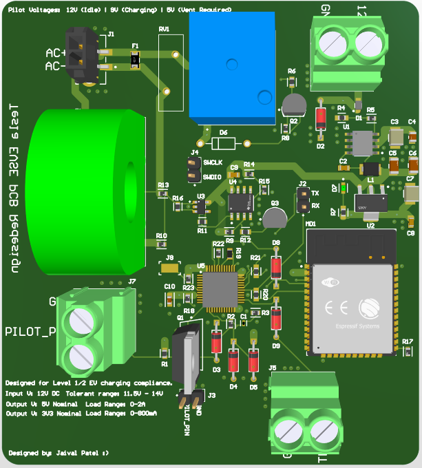
Designed on a 6-layer PCB, the layout optimizes for signal integrity, electromagnetic compatibility (EMC), and thermal management. Layer partitioning separates power planes for 3.3V and 12V operation while providing solid return paths and shielding for digital and analog signals. Diagnostic feedback is logged and transmitted over BLE, enabling mobile app or desktop-based monitoring—a significant step toward connected EVSE infrastructure.
This project not only addresses the limitations of existing open-source designs but modernizes the EVSE architecture to align with Tesla-grade standards. It provides enhanced safety logic, embedded BLE stack integration, and future extensibility for cloud-based telemetry, remote diagnostics, and smart charging algorithms.
Key Features & Design Decisions
The Tesla-Grade BLE EVSE Board was architected from first principles to improve upon the open-source OpenEVSE schematic and bring charging system control up to modern automotive-grade standards. Each subsystem—ranging from signal sensing and relay actuation to fault detection and wireless diagnostics—was selected and refined to ensure safety, modularity, robustness, and extensibility for next-generation vehicle charging workflows.
STM32 Microcontroller Core
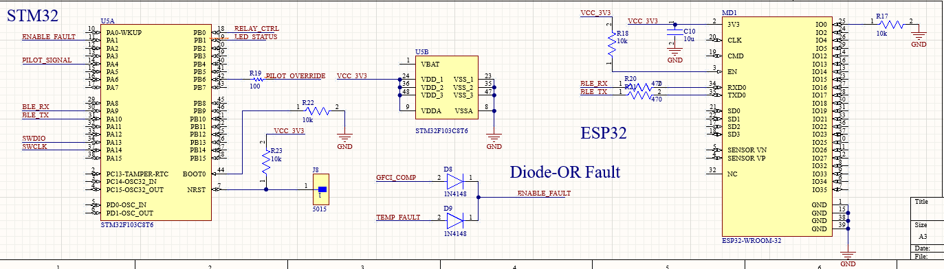
The STM32F103C8T6 was chosen as the control core for this EVSE board due to its deterministic real-time performance, built-in ADCs, USARTs, GPIO flexibility, and proven reliability in embedded automotive applications. Its 72 MHz Cortex-M3 core allowed us to implement a clean finite-state machine (FSM) that governs the J1772 state transitions:
- State A: No vehicle connected
- State B: Vehicle detected
- State C: Vehicle requesting charge
- State D: Ventilation required
- State E: Fault or error
By using timer interrupts and analog read thresholds, the microcontroller continuously monitors the pilot signal, ground continuity, and temperature sensors. The FSM transitions trigger actions like relay enable, BLE alert, or system shutdown. The STM32's low-power modes were also evaluated for future versions that may operate intermittently from solar or off-grid sources.
BLE Telemetry via ESP32-WROOM-32E
BLE-based diagnostics were added to modernize the EVSE interface and allow real-time communication with mobile or desktop apps. The ESP32-WROOM-32E module was selected for its robust BLE stack, UART/ADC interfaces, and compatibility with over-the-air (OTA) updates. Communication between the STM32 and ESP32 is UART-based with a shared protocol layer for:
- State reporting (FSM transitions, charge active, fault status)
- Temperature and pilot signal telemetry
- Relay on/off command logging
BLE integration enables features typically unavailable in traditional EVSEs—like usage history, predictive diagnostics, and remote lockout. It also facilitates secure firmware debugging without physical access to the charger internals.
Pilot Signal Detection Circuitry
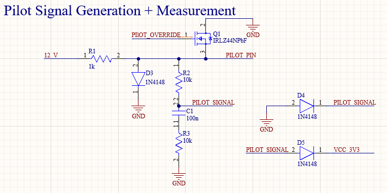
Pilot signal detection is the heart of EVSE logic. The pilot is a ±12V PWM waveform sent by the EVSE and measured back by the vehicle to signal its readiness. We implemented this sensing path using a precision voltage divider, low-pass filter, and op-amp buffer, feeding into the STM32 ADC. This allowed robust reading of voltage levels and accurate duty cycle capture, used to determine:
- Vehicle presence (valid ±12V swing)
- Charging current limit (based on PWM duty cycle)
- Error or ground fault conditions
The analog front-end was carefully matched to handle both the bipolar signal range and the low-noise filtering required for proper FSM decoding under noisy environmental conditions.
Relay Control & Enable Signal Conditioning
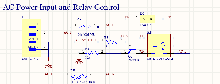
The high-voltage relay that energizes the charging line is controlled through an N-channel logic-level MOSFET, driven by the STM32. A flyback diode and snubber network are included across the relay coil to suppress inductive transients, ensuring long-term component health and compliance with electromagnetic emission standards. The system architecture includes:
- Signal inverter buffer before MOSFET gate (optional)
- Relay active-status feedback to STM32 (via voltage divider)
- Current path rated for high surge withstand (relay selected accordingly)
This design guarantees that relay activation is tightly controlled and monitored, preventing unexpected activation during faults or communication errors.
Temperature Fault Detection (TEMP_FAULT)
An analog comparator circuit compares a thermistor divider to a reference threshold. If the sensed temperature exceeds a safe level (typically 70–80°C), the comparator outputs a LOW signal which triggers a system-wide shutdown. This TEMP_FAULT signal is diode-ORed with other fault conditions (e.g., GCP_COMP) to enforce the following:
- Automatic disabling of relay enable signal
- LED status indication (overheat condition)
- BLE fault broadcast
By isolating this signal in hardware, we achieve a fail-safe shutdown mechanism independent of firmware responsiveness. This is a critical requirement in automotive-grade EVSEs to prevent connector damage or user injury.
Ground Continuity Protection (GCP_COMP)
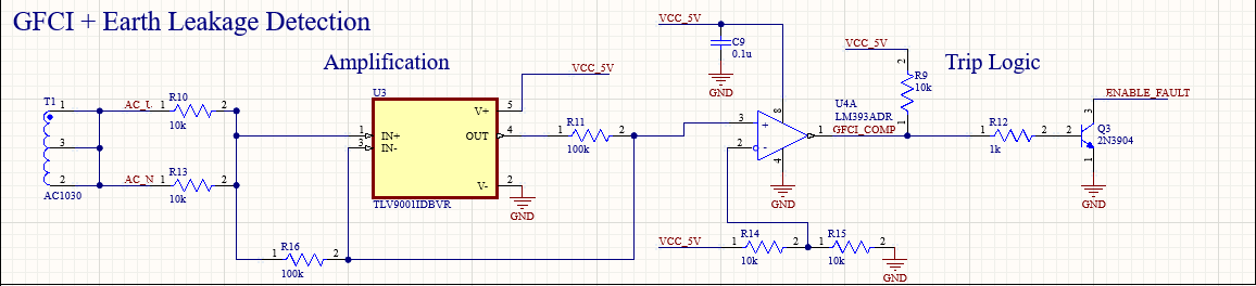
Ground continuity is critical for safe EV charging. GCP sensing is implemented using a voltage divider between pilot and ground routed into a comparator (e.g., LM393). If the voltage drops below a minimum expected threshold, GCP_COMP is pulled LOW. This line feeds into the same diode-OR fault network, disabling the relay and alerting the system.
This setup is aligned with best practices in EVSE design and validates proper earth connection to the vehicle chassis. It is particularly useful in field-deployed chargers exposed to high-impedance ground loops or corroded connectors.
Diode-OR Fault Logic (ENABLE_FAULT)
ENABLE_FAULT is the output of a diode-OR network combining TEMP_FAULT and GCP_COMP lines (view Figure 1). When any of the two signals is asserted LOW, ENABLE_FAULT also goes LOW, which disables the DRV (relay driver). This hardware-level logic is implemented using 1N4148 switching diodes and a pull-up resistor. The line then drives:
- An NPN transistor (Q1) which sinks relay enable current
- A red LED for visual indication of fault condition
This circuitry was chosen over software-based fault shutdown because it provides sub-millisecond response time, isolating the fault path from firmware logic and ensuring robust operation under corner-case transients.
Power Regulation Architecture
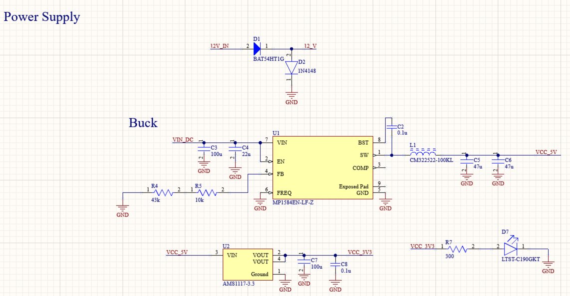
The EVSE operates from a wide-range DC input (typically 12V–24V), supplied via barrel jack or XT60 connector. The board includes:
- 3.3V Rail: Generated using an AMS1117-3.3 LDO. Used for STM32, ESP32, and BLE stack peripherals. The regulator was selected for its simplicity and ability to supply 800mA peak current—sufficient for low-power embedded tasks.
- 12V Rail: Direct input or created using a step-up topology (TPS6104 or similar) in future versions for auxiliary needs.
- TVS + Reverse Polarity Protection: Series diode and 5V clamping TVS diode were added to protect the board from voltage spikes and incorrect barrel jack connections.
Each regulator is bypassed with ceramic capacitors (0.1µF + 10µF) and polyfuse-protected to contain shorts. Power domains were separated by ferrite beads to reduce noise coupling.
9. LED Status Indicators
To assist debugging, three LED indicators were added:
- POWER: Indicates 3.3V system rail active
- RELAY: Indicates high-voltage relay is energized
- FAULT: Indicates ENABLE_FAULT condition is active
These allow installers and developers to visually assess board health and fault status without needing external instruments.
BLE Debug Commands & Logging
BLE command handlers were implemented in the ESP32 firmware to support diagnostics:
- Request current FSM state
- Query last fault condition
- Read PWM duty cycle from pilot signal
- Enable/disable relay manually
These features offer significant convenience during bring-up and field testing, and may be expanded into mobile app-based controls.
PCB Layout Strategy
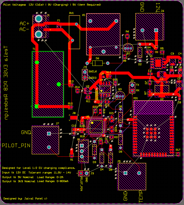
The layout of the Tesla-Grade BLE EVSE board was guided by principles of electrical isolation, thermal robustness, signal clarity, and EMI reduction, all while achieving a compact and modular form factor. This section outlines the rationale behind the placement of subsystems, layer stackup design, trace routing, grounding philosophy, and EMI containment—all crucial for high-reliability automotive charging environments.
1. Layer Stackup Rationale
A 6-layer PCB architecture was used with the following structure:
- Layer 1 (Top): Power traces + component placement
- Layer 2: Power (3.3V polygon pour)
- Layer 3: Power2 (used for 12V routing and wide-pour shielding)
- Layer 4: Signal (high-speed UART, ADC, and pilot signal routes)
- Layer 5: Signal2 (pilot return paths, debug UART, and enable line)
- Layer 6 (Bottom): Solid GND plane with via stitching
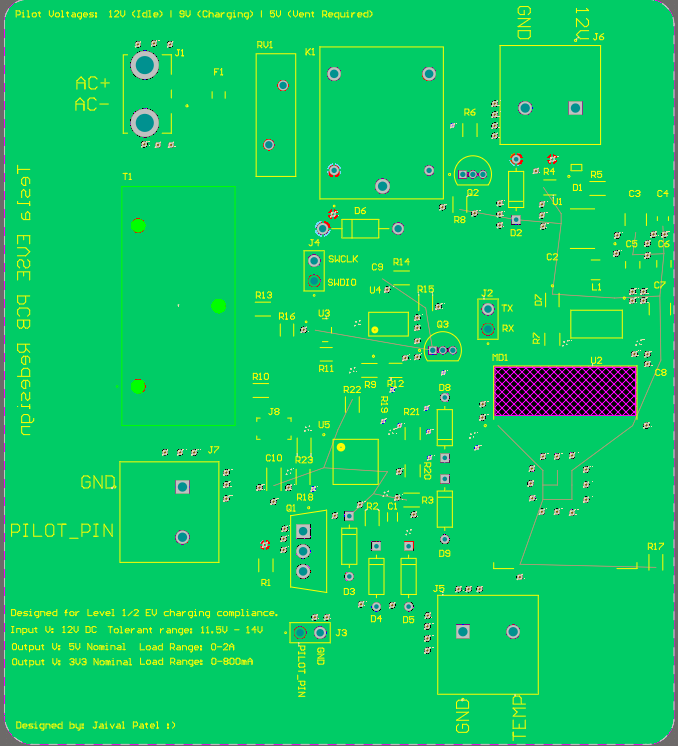
This stack was selected to enable effective vertical separation of sensitive analog signals (e.g. pilot detection) from high-power or switching nodes (e.g. relay coil and power input). The use of dual internal power planes allows distributed decoupling without compromising trace impedance control.
Analog vs Digital Domain Partitioning
The analog pilot signal front-end and temperature sensing logic were physically separated from the digital FSM and BLE telemetry logic. The STM32 sits near the digital center of the board, flanked on one side by the analog front-end (e.g., pilot buffer, comparator, temperature fault logic) and on the other by the UART connection to the ESP32.
A moat-like ground isolation approach was used: a continuous copper pour surrounds the analog front-end and connects to the global GND only via a single-point ferrite bead near the STM32 AGND pin. This topology avoids ground loops and prevents digital switching noise from contaminating pilot signal ADC reads.
BLE Module Placement & Routing
The ESP32-WROOM-32E was placed at the top right edge of the board to expose the onboard PCB antenna to free air, reducing RF interference. The UART TX/RX lines to the STM32 were routed on inner layers with consistent spacing and shielding via adjacent ground copper. A keepout zone was declared below the antenna and on the top layer copper to preserve antenna radiation pattern and BLE signal range.
Additional care was taken to separate noisy switching circuits (relay coil, DRV gate driver) from the BLE module’s 3.3V supply rail, using ferrite bead isolation and localized decoupling (10µF + 0.1µF).
Power Distribution & Protection Layout
Power entry occurs at the top-left XT60 connector, with wide 100 mil traces routing 12V to the relay and 3.3V regulators. The AMS1117-3.3 was placed directly adjacent to the STM32 to reduce IR drop and suppress load transients. Output capacitors were placed within 2 mm of the LDO VOUT pin and mirrored underneath with stitched vias to GND for optimal return current.
The diode-OR fault shutdown logic (ENABLE_FAULT) was routed close to the relay MOSFET and STM32 output pin to minimize propagation delay. Pull-up resistors and the transistor base bias resistor were co-located with the Q1 shutdown transistor, ensuring layout-induced signal reflection was minimized.
Pilot Signal Conditioning Path
The pilot signal detection path follows this chain: pilot → resistor divider → filter cap → op-amp buffer → STM32 ADC pin. This entire chain was routed on the inner Signal layer with a continuous reference GND underneath. Sensitive nodes (e.g., filtered midpoint) were shielded with grounded copper pour and surrounded by analog GND stitching vias for protection against ambient RF.
The comparator outputs (TEMP_FAULT, GCP_COMP) were routed on Layer 4 directly into the diode-OR fault logic zone, avoiding any crossover with high-current relay lines or PWM outputs.
Relay Control Circuit & High-Current Path
The N-channel MOSFET controlling the relay was placed near the relay coil with wide 70 mil traces connecting to the 12V high-current plane. A flyback diode (1N5822) was placed as close as possible across the coil terminals to clamp inductive spikes. All control signals were routed on inner layers, isolated from the relay power paths.
The ground return from the relay coil was routed directly into the solid GND plane via a dedicated low-inductance path, avoiding interaction with analog or digital ground returns.
Debug Interfaces & Programming Headers
The SWD programming header for the STM32 and UART breakout for ESP32 debugging were placed at the board edges for tool-free access during bench testing. Both were surrounded by GND copper zones and labeled clearly via silkscreen. Series resistors (10Ω) were added to prevent line ringing on high-speed SWDIO/SWCLK lines.
Fault Logic Placement & Visualization
The TEMP_FAULT and GCP_COMP comparators, along with the ENABLE_FAULT logic and transistor switch, were grouped into a cohesive sub-circuit near the relay gate driver. This allowed tight coupling between:
- Fault detection signals
- Shutdown gate signal to DRV
- FAULT LED indicator
The red LED is current-limited via a 330Ω resistor and positioned on the top right corner of the board for clear visibility inside enclosures.
Ground Plane Strategy & EMI Mitigation
As seen from Figure 10, Layer 6 (Bottom) is a continuous solid GND plane stitched liberally with vias from all decoupling caps and connectors. GND stitching vias were placed:
- Along the perimeter of the board (every 5 mm)
- Underneath every bypass cap pair
- Between analog and digital domains to form a fence
This extensive ground network lowers loop inductance and provides effective shielding against radiated emissions. Additionally, power trace loops were minimized by placing decoupling caps adjacent to supply pins and using short, wide traces.
10 Thermal Planning
While this board handles low-to-moderate power loads ( less than 1A typical), thermal relief was added to the AMS1117 LDO and relay MOSFET zones. Copper planes on Layers 2 and 3 were used as heat spreaders. Thermal vias were stitched around the LDO to aid passive dissipation, and the relay was spaced to avoid coupling into adjacent low-power ICs.
The Tesla-Grade BLE EVSE PCB layout exemplifies principles of clean system partitioning, EMI-resilient design, and real-world maintainability. Every signal path—from BLE telemetry and STM32 control to fault isolation and analog sensing—was routed with purpose. Compared to the original OpenEVSE layout, this version enhances electrical integrity, improves safety isolation, and supports modern wireless debugging workflows—making it suitable for real deployment in robotic test chargers, EV development benches, and automotive R&D settings.
Challenges & Future Work
Design Constraints and Trade-offs
While the final board demonstrates robust telemetry, safety logic, and charging control, several key design challenges were encountered during development. These included power domain isolation, BLE signal integrity, thermal considerations around the AMS1117 LDO, and tuning fault propagation delay between comparator outputs and DRV shutdown logic.
1. BLE Interference and Antenna Isolation
The ESP32-WROOM-32E’s onboard PCB antenna required a strict keepout zone and physical separation from switching noise sources such as the relay gate driver and PWM-controlled DRV signals. Despite placing the module near the board edge, EMI coupling through shared 3.3V rails caused intermittent telemetry dropouts during high switching activity. This was mitigated with local decoupling (10μF + 0.1μF) and ferrite bead filtering (600Ω@100MHz) but future designs may benefit from an external ceramic antenna or shielded module.
2. Grounding Complexity
Achieving effective analog/digital ground separation without introducing ground loops was non-trivial. Early revisions suffered from ripple injection into the pilot ADC due to shared return paths with USB UART lines. This was corrected by restructuring the GND plane and introducing analog-GND stitching only at the STM32 AGND pin via a ferrite bead. Even so, maintaining low-impedance return paths under dynamic loads remains a priority in future layouts.
3. AMS1117 Heat Dissipation
Though the AMS1117-3.3 was chosen for its simplicity and availability, its linear nature led to significant heat buildup when sourcing over 200 mA—particularly during BLE transmission spikes and USB logging. The addition of copper flood heatsinking and thermal vias helped dissipate heat, but active regulation (e.g., switching buck converters) will be evaluated in next iterations to reduce thermal stress and improve battery efficiency.
4. DRV Gate Control Race Conditions
The ENABLE_FAULT signal, derived from diode-OR logic combining TEMP_FAULT and GCP_COMP, controls the DRV8353’s ENABLE pin. However, initial testing revealed microsecond-scale race conditions when both comparators toggled simultaneously. This was traced to slow rise/fall times through the diode logic and insufficient pull-down strength on the transistor gate. Series resistance tuning and stronger pull-ups were introduced, but future revisions may use a logic buffer or dedicated fault controller IC to guarantee edge cleanliness.
5. Mechanical & Debug Accessibility
Because the BLE EVSE board is intended for embedded use in constrained test rigs, physical access to the SWD header and UART debug lines was critical. During initial bring-up, dense trace routing around the STM32 limited the accessibility of these headers for probe clips. The final layout pushed these headers to the board edge, but future revisions may introduce a debug mezzanine or snap-off section to preserve mechanical integration while retaining access.
Future Improvements
The Tesla-Grade BLE EVSE board is deployment-ready, but several upgrades are planned to extend its performance and field usability:
- Switching Regulators: Replace the AMS1117 with a buck regulator (e.g., TPS62125) to reduce power loss and improve efficiency under BLE loads.
- BLE Firmware Enhancements: Extend the ESP32 firmware to support OTA updates, encrypted telemetry, and adaptive advertising based on fault state.
- Wireless Power Integration: Combine with a future QiBridge receiver board to explore BLE-based contactless charging modules with full telemetry feedback.
- CAN-FD Telemetry Expansion: Introduce an optional CAN-FD transceiver to support automotive bus diagnostics alongside BLE, useful in hybrid or dual-stack development settings.
- Sensor Expansion: Add hall sensors or current sense amplifiers (e.g., INA240) to validate actual relay load behavior and implement closed-loop fault prediction.
- Conformal Coating & Assembly: Use automotive-grade soldermask, silkscreen labeling, and pre-applied conformal coating to support field deployment in harsh environments.
Reinforcement Learning for Embedded EV Charging Control
This project implements a Proximal Policy Optimization (PPO)-based reinforcement learning controller for a custom EVSE (Electric Vehicle Supply Equipment) system. The agent learns to toggle the relay based on temperature and pilot signal feedback, optimizing for safe, fault-free charging while running entirely on embedded hardware.
Both the paper and model repo can be found in the links above.
System Overview
- Microcontroller: STM32F103C8T6
- Telemetry: BLE (ESP32-WROOM-32E)
- Inference: Quantized TFLite model deployed via TensorFlow Lite Micro
- Inputs: Pilot signal status, relay state, internal temperature, and fault flags
- Outputs: Relay control signal and BLE telemetry for rollout monitoring
Environment & Reward Design
The EVSE environment simulates thermal dynamics, relay-induced heating, and fault zones using a 4D observation space. PPO is rewarded for charging safely (+2.0) under temp < 0.9, lightly penalized for risky behavior, and heavily penalized (-10.0) when a fault occurs. A fault-aware policy emerges that balances long-term safety and energy efficiency.
Training Pipeline
The PPO agent is trained for 500,000 steps in Gymnasium using Stable-Baselines3. Random initial states and stochastic temperature dynamics encourage robustness. The final policy is exported to ONNX, converted to TFLite, and quantized to 8-bit for deployment.
Deployment
The model is run on the STM32 microcontroller with inference every 100 ms. Relay control is updated based on the PPO action output, and BLE transmits rollout data for live visualization. The full deployment pipeline fits within 30 KB flash and runs under 100 ms latency per cycle.
Evaluation & Results
- Reward Gain: PPO achieves 2.3× higher reward than heuristic and 3.1× over random policies
- Ablation Resilience: Robust to connector dropouts and hot starts, sensitive to sensor noise
- Fault Avoidance: Maintains temperature
< 0.95in over 98% of rollouts - Deployment Footprint: 28 KB quantized model; less than 80 ms average inference time
This project demonstrates safe, real-time control with embedded reinforcement learning on a low-power microcontroller. It replaces rule-based EVSE firmware with an adaptive policy that learns from environmental interaction, respects physical safety limits, and generalizes across perturbations. The full stack — from simulation to STM32 deployment — showcases how RL can unlock new capabilities in autonomous embedded energy systems.