TracLink PDU
Overview
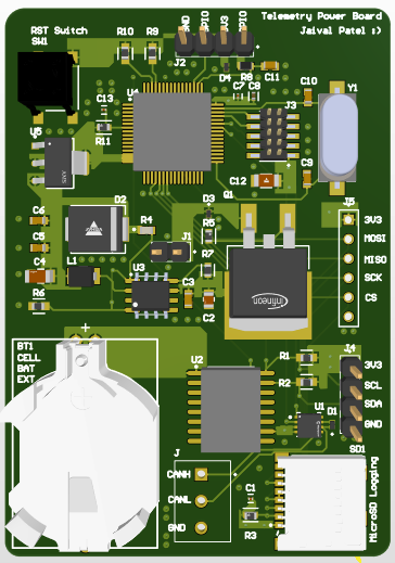
The Telemetry Power Hub project was conceived as a critical interface between onboard vehicle sensors and the data acquisition system in a high-performance endurance racing environment. This system demanded a reliable, efficient, and noise-resilient interface to power, aggregate, and transmit sensor signals under severe thermal and mechanical constraints. The central design objective was to enable seamless telemetry support with modularity, minimal power loss, and future scalability. The system needed to withstand engine bay-level heat, vibrations from prolonged operation, and provide real-time diagnostics through CAN interfacing.
Key Features
CAN Interface
The decision to integrate a robust Controller Area Network (CAN) interface was driven by its resilience in noisy environments and its widespread adoption in motorsports for distributed communication. A TI SN65HVD230DR transceiver was chosen due to its extended temperature range (-40°C to 125°C), integrated TXD/RXD loopback, and protection against differential bus shorts. Unlike alternatives like MCP2551, the SN65HVD230 offered better EMC performance with lower power consumption and failsafe dominant-recessive control logic. This selection ensured high-fidelity communication across the noisy automotive environment without compromising data integrity.
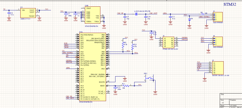
STM32 Microcontroller:
The STM32F103C8T6 was selected due to its proven track record in embedded control systems, offering a balanced mix of performance (72 MHz Cortex-M3), power efficiency, and a rich peripheral set (including CAN, UART, SPI, I2C, ADCs, and timers). Unlike higher-end STM32H7 devices, the STM32F103C8T6 fit the budget and power profile while meeting all firmware control and logging requirements. It also enabled compatibility with existing race firmware libraries already used by other teams, easing integration and debugging.
Power Regulation Strategy:
A modular dual-rail system was adopted for providing 5V and 3.3V lines from a single LiPo battery pack input (nominal 7.4V). The AP2112K-3.3 LDO regulator was chosen for analog rails due to its low dropout voltage and excellent PSRR, essential for minimizing ripple into sensitive sensor ADC inputs. For higher power domains like digital logic and sensor buses, the MP1584EN buck regulator was used. It supports up to 3A continuous load current, high switching frequency (up to 1.5 MHz), and built-in thermal/current protections. Other candidates like LM2596 were discarded due to their bulkier footprint and lower efficiency at low load currents.
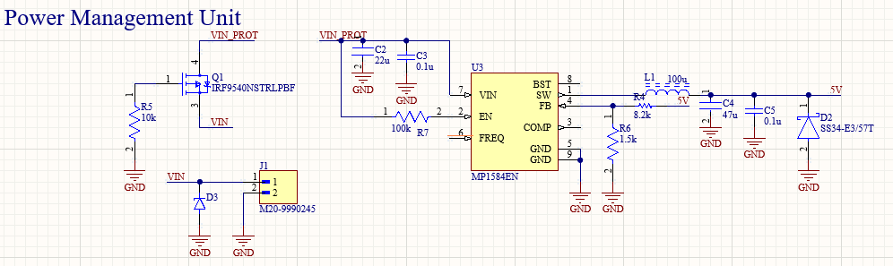
Buck Regulator Implementation:
The MP1584EN design required careful selection of external components to stabilize transient response and reduce switching noise. A 22µH inductor and 47µF output capacitor were selected after load-line analysis. The switching node layout was minimized to avoid radiation loops, and feedback lines were routed separately from high-current paths. The inductor's DCR was optimized for thermal performance given the limited copper area. The layout respected the manufacturer’s recommendations for thermal vias under the exposed pad to dissipate heat effectively, even under peak draw from sensor arrays.
Sensor Interface Design:
The analog sensor ports were provisioned as universal headers with optional pull-ups and anti-aliasing RC filters. Separate ports were assigned for I2C and SPI sensors, each routed with impedance-controlled traces and low-side ESD diodes to mitigate damage from miswired connections. The threshold resistors for logic level compatibility (e.g., 5V sensor to 3.3V MCU) were dimensioned through SPICE simulations to ensure rise time compliance across the full sensor cable length, which was estimated to vary from 20 to 80 cm depending on deployment zone in the vehicle.
Modular Expansion Capability:
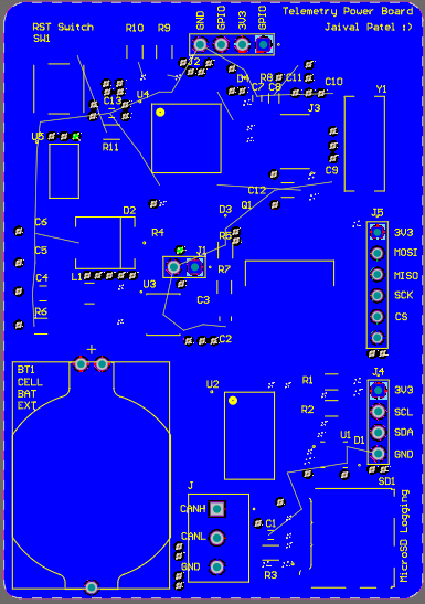
Board-to-board headers and redundant bus pinouts were included to allow for future telemetry module attachment or daughterboard sensor clusters. The design decisions behind keeping the CAN bus exposed externally (instead of backplane-routed) were guided by serviceability—allowing teams to swap modules trackside without removing the main board.
PCB Layout Strategy
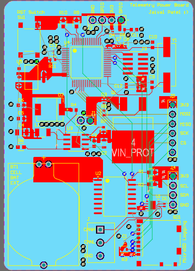
The PCB layout for the Telemetry Power Hub was engineered with multi-domain isolation, EMI robustness, and thermal efficiency in mind. A 4-layer stack-up was used, consisting of the following:
- Layer 1: Signal and Power Routing
- Layer 2: Dedicated Power Plane (3V3)
- Layer 3: Signal and Control
- Layer 4: Signal Plane
- Layer 5: Signal Plane
- Layer 6: Ground Plane
Analog-Digital Isolation:
One of the key layout strategies was segmenting the analog sensor acquisition section from the digital communication and processing blocks. Sensitive analog inputs were routed on Layer 1 with short, shielded traces leading to filtering capacitors and ESD clamps. These were placed close to the edge connectors and fed into low-noise analog LDO rails isolated from digital switching activity by ferrite beads (600 Ohm @ 100 MHz).
Grounding & Return Path Design:
A solid ground plane (Layer 4) spanned the entire board. Star-ground topology was followed at the power connector junction, separating analog and digital domains. Ground stitching vias were placed at high-frequency transition points (near CAN transceiver, switching regulators, and crystal oscillators) to minimize ground bounce and return loop inductance.
Power Distribution & Trace Sizing:
The power input traces from the battery to the MP1584EN regulator were sized for up to 3A load using 40 mil width with a 2 oz copper layer. The 5V rail distribution was done through polygon pours and flooded inner planes (Layer 2), enabling efficient current delivery without voltage drops. Thermal relief was maintained around regulator pads to simplify soldering and avoid cold joints.
Connector Placement & Accessibility:
All vehicle-facing connectors were placed on a single edge of the PCB to allow pit-side cable swaps without disturbing internal mounts. CAN headers were aligned orthogonally to avoid cross-interference with adjacent SPI sensor lines. This orientation also ensured clean mechanical fit within the ECU enclosure mockup used in early testing.
Controlled Impedance Traces:
SPI and I2C signals were routed with matched-length traces, respecting the characteristic impedance (~55 Ohm) of the 4-layer board with FR4 (εr = 4.4). Edge-rate controlled drivers were used on the STM32 to reduce ringing. Ground return traces were run parallel wherever possible, and differential pairs were spaced with 5W:1S ratio for the CAN_H/CAN_L lines.
Decoupling and Bypass Strategy:
Every power pin on ICs had at least one 0.1 µF X7R capacitor placed within 3 mm. Bulk capacitors (10 µF–100 µF) were distributed evenly on each rail and checked for anti-resonance overlaps via impedance spectroscopy simulation. Each regulator had an input cap and a ferrite bead to damp input voltage fluctuations.
Heat Management & Via Stitching:
The buck regulator’s exposed pad was connected to a thermal via array, linked to copper pours on Layer 2 and Layer 4. Additional vias were placed near all high-current traces and near the CAN transceiver IC to sink thermal hotspots. Airflow simulation under CFD revealed no hotspots above 72°C in a fan-cooled environment at 30°C ambient.
Challenges
This project was defined by a unique mix of racing-grade ruggedness and tight electrical tolerances. I encountered the following major challenges during design and prototyping:
Compact Enclosure Constraints The entire board had to fit within a 90mm × 60mm × 20mm space, shared with other control hardware. This necessitated extremely compact layouts and careful avoidance of trace congestion, especially around the microcontroller. The connectors and sensor breakouts also had to be accessible from a single face, reducing freedom for layout routing.
CAN Signal Integrity The CAN lines are notorious for being sensitive to impedance mismatch and stub reflections. Our initial routing led to transceiver malfunctions at 1 Mbps. Only after simulating the trace impedance using KiCad’s stack-up calculator and adjusting trace width + spacing did I stabilize transmission. Adding termination resistors in-line and shielding CAN lines resolved transient spikes seen during ignition startup.
Thermal Isolation The buck regulator’s switching operation caused local hot spots during load spikes from sensors. Given the PCB's enclosure lacked active cooling, I had to use a heavier copper layer (2 oz) and deploy heat-spreading planes under key components. Despite initial layout assumptions, empirical testing forced us to shift the MP1584EN 3mm further away from the STM32 to avoid thermal cross-talk affecting the crystal oscillator.