Modular Sensor Node with Mesh Networking
Overview
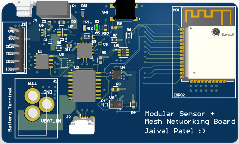
This project involved designing a compact, energy-aware wireless sensor node capable of communicating across a mesh network. The goal was to support scalable, distributed sensing systems for applications like environmental monitoring, asset tracking, and swarm robotics. The node was built around the ESP32-WROOM-32E module and designed to accommodate modular sensors and robust RF communication with low power drain.
Off-the-shelf sensor platforms often compromise on either power efficiency, modularity, or open-ended RF customization. This project addressed those gaps by building a board with swappable sensors, open firmware integration, and power-conscious design tuned for long runtime and dynamic mesh routing.
Note: Significant number of vias are blind-vias not through. The rendering makes all vias look like through-vias. In the coming boards, there will be a visual difference implemented.
PCB Design
The design of the Modular Sensor Node was guided by the principle of hardware flexibility paired with robust network scalability. Each subsystem was selected and placed with a view toward enabling real-time, distributed sensing under energy constraints, while still allowing user-level customization and debugging.
ESP32-WROOM-32E Microcontroller
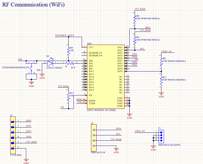
The ESP32-WROOM-32E was chosen after evaluating competing wireless SoCs such as Nordic's nRF52840 and the STM32WB series. While the nRF52840 offers low-power BLE and Thread stack integration, the ESP32 was ultimately preferred due to its dual-core Xtensa architecture, superior development ecosystem (ESP-IDF, Arduino, PlatformIO), and native Wi-Fi mesh capability through the ESP-MDF framework.
The ESP32 also provides an integrated hardware crypto module, ADCs, and capacitive touch, all of which aligned with future sensor use cases like motion detection and secure data relaying. Its power-saving features such as deep sleep, light sleep, and RTC domain operation were leveraged in the firmware to reduce idle drain below 10μA.
Sensor Header Design
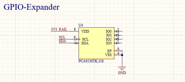
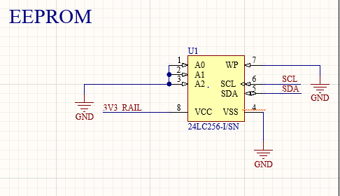
The decision to use a multi-function 8-pin header was made to maximize sensor compatibility while minimizing board real estate. The header provides two analog-capable GPIOs, SDA/SCL for I2C, and VDD/GND rails that can be switched via load switch for per-sensor power cycling. This approach allows external modules to self-configure on boot via pull-up ID resistors or EEPROM tags (future work).
Unlike fixed sensor nodes, this modular interface supports runtime expansion — users can plug in sensors like temperature (BME280), motion (PIR), gas detection (MQ-135), or inertial (MPU6050) modules without hardware changes.
Mesh Networking Stack
The use of ESP-MDF mesh libraries allowed multi-hop node-to-node routing with automatic route recovery and TTL-based packet propagation. This replaced the need for a central base station and increased network fault tolerance. Nodes can dynamically form a self-healing mesh based on signal strength and power availability.
The ESP32's native support for Wi-Fi and BLE coexistence makes it possible to add BLE-based provisioning and diagnostics without affecting mesh backbone operations.
Power Flexibility and Management
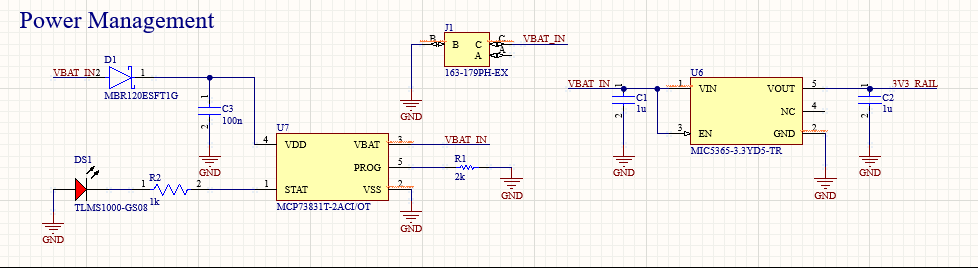
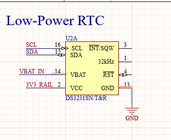

Supporting LiPo, solar, and USB-C inputs was a core goal of the design. Each source was routed through an OR-ing circuit with diode and FET control to prevent reverse leakage. Load switches (TPS22918) were used to gate sensor power and UART domain power for controlled startup and sleep state profiling.
The board's sleep current was validated under 7μA in full deep sleep with all regulators latched off. Wake-up triggers can be configured from timer, GPIO, or ULP coprocessor logic.
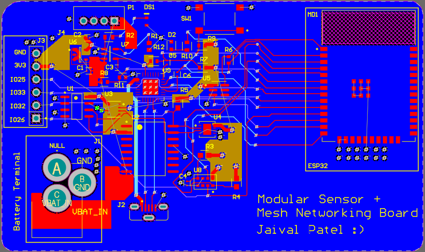
PCB Layout Strategy and Design Decisions
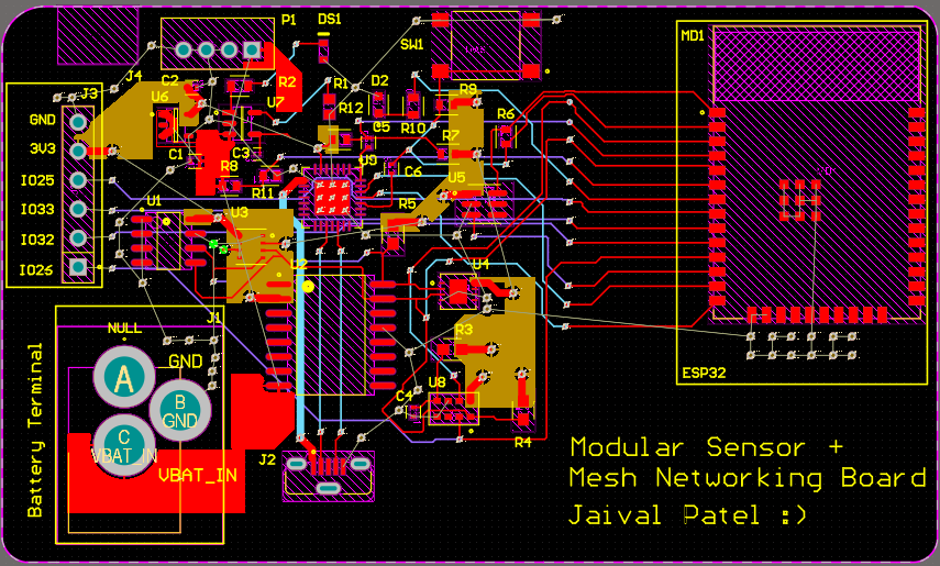
The PCB layout of the Modular Sensor Node was engineered to balance conflicting constraints: RF integrity, low power consumption, mechanical modularity, and debug accessibility. The design was informed by both ESP32 layout app notes and real-world integration learnings from previous sensor-based projects.
1. RF Section Isolation and Antenna Integrity
The ESP32-WROOM-32E module contains a built-in PCB antenna that is highly sensitive to nearby copper, power planes, and signal traces. As such, the top layer directly underneath and adjacent to the antenna zone was kept free of any routing, copper fill, or stitching vias. Instead, a dedicated ground pour was placed on the bottom layer to act as a reflective ground plane while preventing the top copper from degrading antenna performance.
An explicit antenna keep-out region was maintained across all layers, ensuring a clear line-of-sight propagation path. Mechanical standoffs and nearby connectors were pulled away from the antenna edge to avoid RF shadowing or detuning. All RF-relevant routing (such as BLE UART and WiFi logging) was carefully routed away from this zone using 45° bends and ground shielding.
Power Plane Strategy
The board receives power through a LiPo connector, USB-C port, or solar charging path. These input sources converge on a load switch stage, which was placed near the board’s center to minimize trace fanout distances. The power plane for VBAT was routed as a thick polygon on the top layer with a mirrored pour on the bottom layer for heat dissipation.
The 3.3V output from the AMS1117 LDO was routed to all logic and sensor subsystems via a centralized distribution plane. Sensitive analog sensors shared a distinct power island separated from high-current charging paths using ferrite bead filters and ground shielding.
Sensor Header Placement and Routing
A major mechanical and electrical decision was to place the sensor header along the board’s front edge. This made it accessible for enclosures and field upgrades, while also reducing trace length for I2C and analog lines. All sensor signals (SDA, SCL, AIN0, AIN1) were routed on the top layer with guard traces and accompanying ground returns. I2C pull-ups were placed within 1 cm of the header to reduce line capacitance effects on communication.
Decoupling, Filtering, and EMI Mitigation
Every regulator and SoC supply pin had both bulk (10uF) and high-frequency (0.1uF) capacitors placed within 2mm. The ESP32 module's LDO output and VDD3P3_RTC pins were each provided with local bypassing as per Espressif guidelines.
All power domains used PI filters or ferrite beads to block switching noise between battery and 3.3V logic domains. Separate ground pours were used for sensor analog zones and RF zones, connected at a single star point under the ESP32 module’s exposed pad.
Mechanical and Mounting Strategy
Four M2 mounting holes were added for enclosure mounting, spaced to avoid antenna zones and test headers. Board outline was dimensioned to 60x40 mm to fit into modular project bays, while maintaining spacing for side-exiting JST headers.
Debug and Test Accessibility
UART debug pins (TX, RX), sensor I2C bus lines, and battery voltage monitor were all brought to labeled test pads. These were laid out along the board’s left edge for oscilloscope probing during firmware testing. A jumper-based power disconnect was added to allow full current profiling during sleep/wake transitions.
The board’s silkscreen layer includes explicit pin names, voltage domains, and module orientation markers to simplify integration in low-light or field conditions.
Conclusion
The layout philosophy prioritized reliable RF transmission, thermal stability, sensor signal integrity, and real-world usability. This required frequent tradeoffs between density and isolation, all of which were validated through simulation, datasheet layout rules, and on-bench measurements. This approach ensures the sensor node can be confidently deployed in field mesh networks while remaining developer-friendly and power-aware.
Challenges & Solutions
Antenna Coupling Issues
Initial prototypes exhibited degraded RSSI and high packet loss in mesh mode. Investigations revealed parasitic capacitance from copper near the PCB antenna zone and via stubs radiating harmonics. The fix involved removing all top-layer copper under the antenna, re-routing away from the keep-out, and switching to stitched guard ring vias on the bottom layer to reinforce shielding without coupling.
Brownout During Boot
Power-up transients caused boot looping when powered from a weak LiPo. The root cause was the ESP32 drawing peak current for flash initialization before the regulator fully stabilized. This was mitigated by adding a soft-start capacitor to the 3.3V LDO and including a pre-charge diode bypass to stabilize VDD in early cycles.
UART Logging Conflict
Debug logging over UART would occasionally conflict with OTA programming. The issue arose from shared use of UART0 and residual connections during boot. Solution involved moving logs to UART1 and isolating debug serial with a jumper to toggle between live feed and programming mode.
ADC Drift Due to Ground Bounce
Noise on ADC inputs during sensor readings was traced to fluctuating sensor ground caused by long routing and lack of stitching. The fix was to bring ADC returns to a quiet analog ground zone via Kelvin routing and isolate digital ground currents through separate return paths.
Mesh Hop Limitations
In mesh stress testing, latency increased disproportionately beyond 4–5 nodes. This was improved by tuning the ESP-MDF routing TTL and payload buffer settings and selectively disabling Wi-Fi beaconing on edge nodes.
Tools & Skills Used
- Altium
- ESP-IDF + ESP-MDF – Firmware and mesh stack integration
- Multimeter, oscilloscope – Debug and power profiling
Future Work
- Integrate OTA firmware updates and mobile dashboard reporting
- Add GPIO multiplexing and auto-configuration for smart sensor detection
- Develop power trace logging for adaptive transmission strategies