QiBridge - Wireless Power and Data Bridge
Overview
QiBridge is a compact, wireless power and data interface board designed to support the next generation of implantable and wearable neural interface systems. Built around a Qi-standard wireless power receiver and a low-noise, isolated power regulation stage, the board enables contactless energy delivery to embedded systems without physical connectors — ideal for hermetically sealed neurotech devices.
The design integrates a LiPo battery charging circuit, 3.3 V LDO regulator, and custom output headers to bridge Qi-derived power to low-power MCUs like STM32. This architecture is especially well-suited for brain-computer interfaces (BCIs), where minimizing infection risk, improving device longevity, and eliminating mechanical failure points are critical.
QiBridge enables developers and researchers to prototype wireless-powered BCI nodes with simplified bench-to-body transition by replacing traditional USB or pogo pin interfaces with a sealed, wireless coupling.
Key Features
Wireless Power Receiver
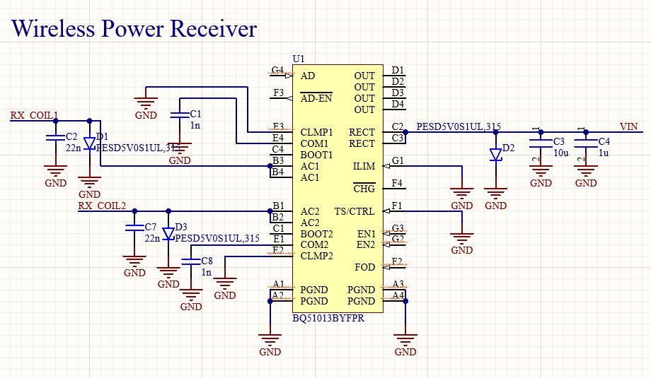
A Qi-standard power receiver IC was selected to enable compatibility with widely available wireless charging pads. This design eliminates the need for physical power connectors and enables applications in sealed or rotating systems. The chosen receiver provided internal rectification, thermal monitoring, and dynamic power negotiation features.
LiPo Battery Charger (MCP73831)
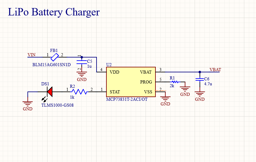
This IC offers a safe and simple way to manage single-cell LiPo charging, with thermal feedback and a regulated 4.2V float voltage. It was selected over buck-based fast chargers due to its small footprint, low cost, and minimal BOM.
3.3V LDO Regulator (AP2112K)
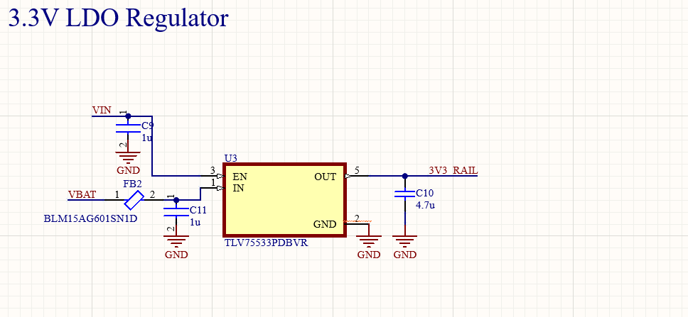
This LDO was selected to generate a clean digital rail for external logic. It features low dropout (typ. 250 mV), excellent PSRR, and is stable with ceramic capacitors. Compared to switching regulators, it significantly reduces noise injection—critical for sensor-driven applications or microcontroller I/O.
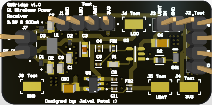
PCB Layout Strategy
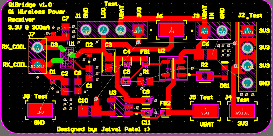
The PCB layout was done in Altium with an emphasis on EMI control and thermal planning. Wide power traces (≥ 50 mils) were used to connect the receiver to the charger and battery terminal. The MCP73831 was placed close to both the receiver output and battery pad to minimize trace inductance.
The LDO output was routed using a star topology to avoid voltage drops between downstream consumers. Bulk ceramic decoupling (10 μF + 0.1 μF) was added close to the output rail and LDO input. To control thermal buildup, a copper fill under the LDO was stitched with thermal vias to bottom ground to increase surface dissipation.
The RX coil area was isolated using a partial ground pour ring, minimizing feedback into the LDO or charging loop. Test points were placed on the regulated output and LiPo terminal for debugging and measurement.
Challenges
Thermal Dissipation: Despite low average current draw, the MCP73831 experienced peak junction temperatures exceeding 60°C during charge. This required layout changes to expose the thermal pad via stitching and reduce trace resistance.
EMI Management: Noise from the inductive receiver introduced ripple on the input rail. Filtering capacitors and layout shielding helped isolate this effect. During testing, ripple was reduced from 180 mV to 60 mV under load.
Space Constraints: The board was limited to under 35 mm × 35 mm. Parts with wide packages or tall profiles (like inductors and LEDs) were minimized to ensure compatibility with embedded enclosures.
Tools & Skills Used
- Altium Designer – schematic capture and 2-layer layout
- LTspice – regulator and charger thermal simulations
- Multimeter, USB PD emulator, thermal IR camera – validation