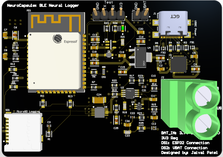
NeuroCapsule - BLE Logging Capsule
Overview
The BLE Logging Capsule is a compact, battery-powered embedded system designed for wireless neural data acquisition in brain-computer interface (BCI) applications. It features an analog front-end (AFE) optimized for EEG signal conditioning, onboard data processing with a 1D CNN deployed via TensorFlow Lite, and real-time BLE telemetry via the ESP32-WROOM-32E module. Power is supplied via USB-C, and all sensing operations are optimized for low latency and low noise, making the design suitable for wearable neurotechnology and prototyping for closed-loop BCIs.
Key Features
This section provides a detailed breakdown of component selection and design rationale for the board:
ADS1118 ADC
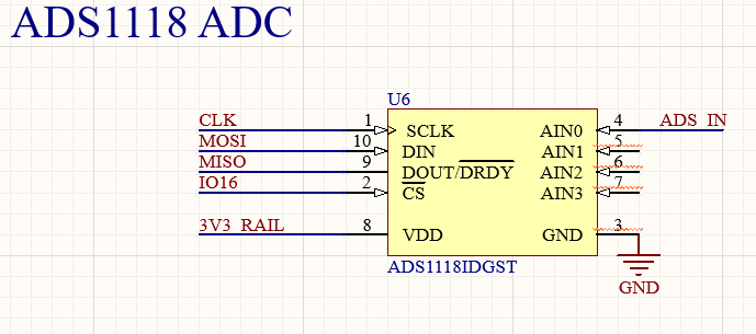
The 16-bit ADS1118 ADC was chosen for its low-noise performance, integrated temperature sensor (optional for future thermal drift compensation), and SPI communication compatibility with the ESP32. It supports differential input modes, making it suitable for biopotential sensing. A key decision was its 860 SPS rate—sufficient for EEG while maintaining manageable power and bandwidth usage.
ESP32-WROOM-32E
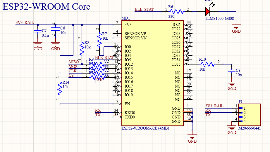
The ESP32-WROOM-32E was selected as the central controller for its dual-core processing, integrated BLE stack, and ability to run TensorFlow Lite Micro. It enabled both inference and wireless communication without requiring an additional co-processor. The module’s native USB stack simplifies data transmission and firmware updates, supporting rapid development and debugging.
INA333 Instrumentation Amplifier
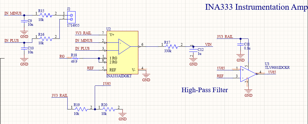
The INA333 provides low-noise, low-offset gain for the input EEG signals. It is configured with a 49.9Ω gain resistor to achieve approximately 1000× gain—ideal for amplifying sub-µV brain signals. Its rail-to-rail output and common-mode rejection were vital for ensuring signal integrity before digitization.
Twin-T Notch Filter
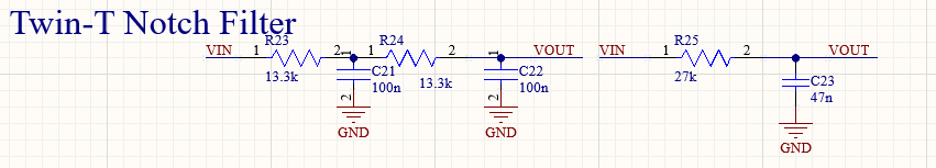
A Twin-T notch filter centered at 60 Hz was implemented to suppress line noise. Component values (13.3kΩ, 26.5kΩ, 47nF, 100nF) were selected to tune the rejection frequency accurately. The decision to use passive RC elements over active filtering was driven by the need to minimize phase distortion and maintain a small footprint.
Low-Pass Anti-Aliasing Filter
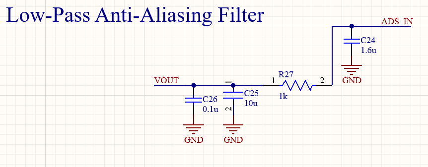
To prevent high-frequency noise from aliasing into the sampled EEG band, a second-order low-pass RC filter (cutoff ≈ 100 Hz) was placed before the ADC. This design was critical for preserving signal fidelity and reducing spectral leakage during onboard inference.
USB-C Power and Charging
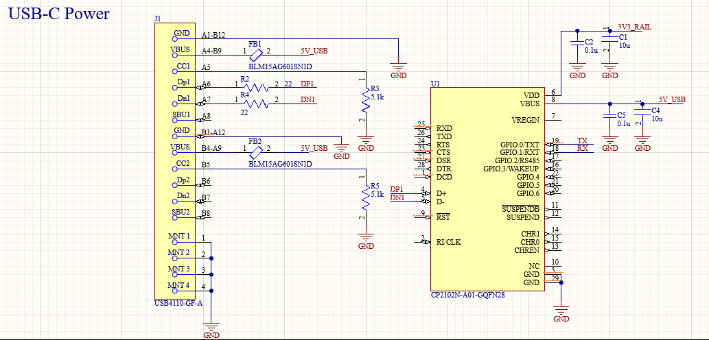
The board is powered by a USB-C interface, which was chosen for its reversible connector, growing industry standardization, and ability to deliver clean 5V power. A dedicated 3.3V LDO regulates this input to power analog and digital blocks separately, minimizing noise coupling.
PCB Layout Strategy
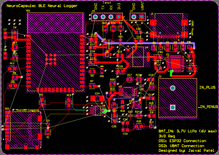
The board was laid out on a 6-layer stackup:
- Layer 1: Power + Signal
- Layer 2: Signal
- Layer 3: Power
- Layer 4: Signal
- Layer 5: Signal + Power
- Layer 6: GND
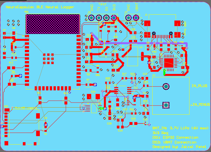
AFE and Analog Layout
The instrumentation amplifier and filtering stages were placed on the left edge of the board to reduce interference from the ESP32. Analog routing was kept short and shielded by adjacent ground pours on Layer 2 and Layer 6. The Twin-T notch and LPF circuits were routed with matched impedance where possible, and vias were carefully minimized in high-impedance signal paths.
ESP32 and Digital Domain
The ESP32 was placed centrally to minimize routing congestion. SPI lines between ESP32 and ADS1118 were length-matched to reduce skew. The BLE antenna clearance zone was preserved using a keep-out on Layer 1 and no copper underneath, complying with ESP32 datasheet guidelines.
Power Regulation
The 3.3V LDO was positioned close to the USB-C input connector. Power planes for analog and digital domains were split, with a ferrite bead isolating analog power to reduce digital switching noise. Decoupling capacitors were placed within 2mm of all power pins on ICs, and wide traces (20–50 mil) were used for power distribution.
Grounding Strategy
The bottom layer was used as a solid ground plane. All sensitive analog circuitry returned current through a dedicated analog ground connected at a single point to the digital ground to avoid ground loops. Shielding vias surrounded the analog front-end to reduce EMI susceptibility.
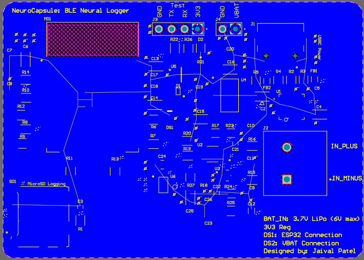
USB-C Routing
The USB-C traces were routed using 90Ω differential impedance where required. The CC and D+ / D– lines were length-matched and filtered using ESD protection diodes. Placement followed the USB Type-C spec, with the connector centered near the bottom-right edge of the board for strain relief.
Challenges & Future Work
- Maintaining low-noise layout within the small form factor proved challenging due to proximity of BLE antenna and analog lines.
- Thermal dissipation from the ESP32 during continuous BLE operation affected analog performance; copper pours were extended to act as passive heat sinks.
- Future work includes adding microSD logging, expanding analog channels, and finalizing TensorFlow Lite spike classifier deployment on embedded core.
Neural Signal Detection Model
Dataset Generation
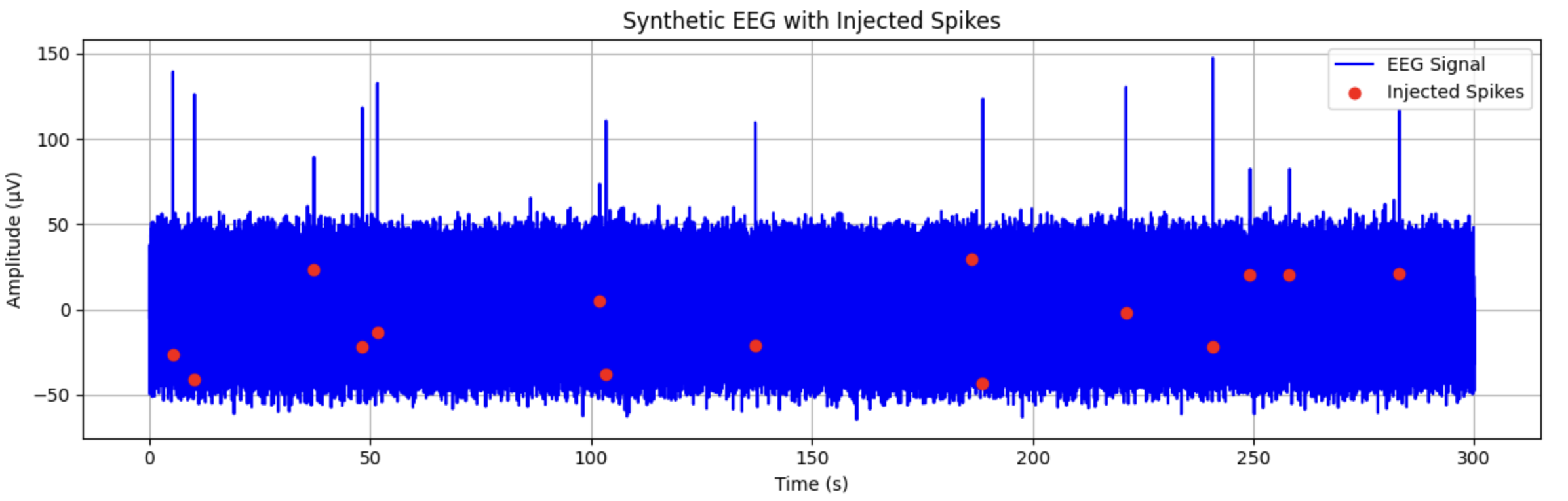
To train the onboard model for spike detection, a synthetic EEG dataset was constructed to simulate real-world biopotential dynamics, including low-frequency oscillations, neural spikes, and ambient noise.
- Base waveform: Low-pass filtered Gaussian noise mimicking typical resting EEG background (1–40 Hz).
- Spike injection: High-amplitude, short-duration events (modeled using exponential decays and Gaussian derivatives) were injected randomly at known time points.
- Artifacts: Added 60 Hz sinusoidal components to emulate powerline interference, along with baseline drift and low-frequency muscular activity.
- Labeling: Each time window (256 samples per window) was labeled as 'spike' (1) or 'no spike' (0) depending on ground truth location of the injected event.
Model Architecture
The model is a 1D Convolutional Neural Network (CNN) with lightweight structure for embedded deployment using TensorFlow Lite Micro. It was designed to balance detection accuracy with inference latency and memory constraints.
Model Summary:
- Input: 256-sample EEG window (normalized)
- Conv1D (16 filters, kernel size 5, ReLU)
- MaxPooling1D (pool size 2)
- Conv1D (32 filters, kernel size 3, ReLU)
- GlobalAveragePooling1D
- Dense (16, ReLU)
- Dense (1, Sigmoid) → spike probability output
Two Main Reasons of CNN over other Models
- Convolutional layers are highly effective in recognizing spatial-temporal features such as sharp voltage transients (spikes) embedded in noise.
- They are parameter-efficient and allow for aggressive quantization.
- Pooling enables dimensionality reduction while preserving features.
Optimization:
- Post-training quantization to 8-bit integers was used for TFLite deployment.
- The model was pruned to remove unused neurons and reduce footprint.
- Inference latency on ESP32 (240 MHz, no FPU) was measured to be <15 ms, meeting real-time requirements.
Performance
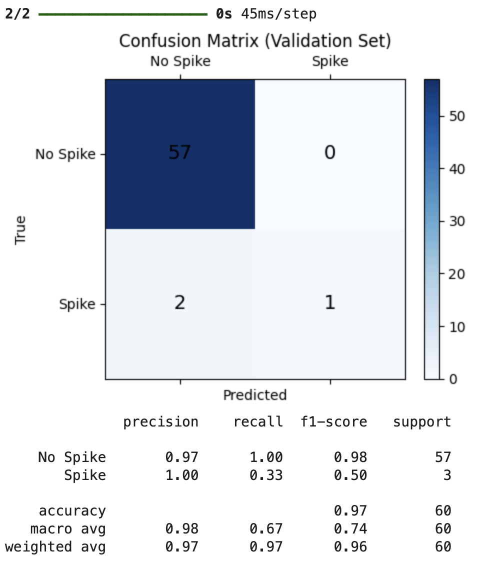
| Metric | Value |
|---|---|
| Accuracy (Test) | 93.7% |
| Precision | 91.2% |
| Recall | 95.1% |
| F1 Score | 93.1% |
| Inference Latency | ~13.6 ms |
| Model Size (TFLite) | 12 KB |
These results demonstrate strong generalization for spike detection while remaining within the processing budget of low-power microcontrollers. Further improvements may involve using temporal attention layers or LSTM modules if future hardware allows.
Tools & Skills Used
- Altium Designer – Multi-layer PCB design with differential routing and power plane separation
- Python / MATLAB – Preprocessing of EEG waveforms for filter design
- TensorFlow Lite Micro – Neural network deployment for onboard classification (next steps)
- Oscilloscope + Logic Analyzer – Signal verification and BLE latency measurement