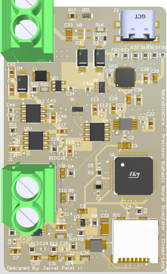
NeuroStimCore - Precision Biphasic Neural Stimulator
This project introduces a wearable, medical-grade embedded system designed for high-fidelity biopotential monitoring with onboard logging, fault detection, and telemetry capabilities. Built around the STM32F103C8T6, the sensor node integrates a precision analog front-end, programmable digital processing, and a robust power architecture that supports standalone operation in clinical and neurotechnology environments. The system includes an instrumentation amplifier (INA333), analog multiplexers, Twin-T notch filtering, low-pass anti-aliasing, real-time clock with logging, and a compact, battery-powered form factor with isolated power rails.
Key Features
Instrumentation Amplifier – INA333
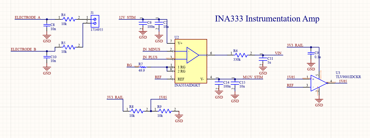
I chose the INA333 because of its low input offset voltage (25μV typ), ultra-low input bias current (200pA), and rail-to-rail output swing. This makes it ideal for EEG and other biopotential sensing applications, where signal amplitudes are often in the range of tens of microvolts. The gain of the amplifier is set using:
Gain = 1 + (50,000 / RG)
I used a 49.9Ω resistor, targeting a gain of approximately 1001×. This brought sub-100μV signals into the millivolt range suitable for 16-bit ADC sampling. Other options like the INA128 were considered but ruled out due to higher power consumption and input offset.
DAC Buffer Architecture – AD5689R + OPA280
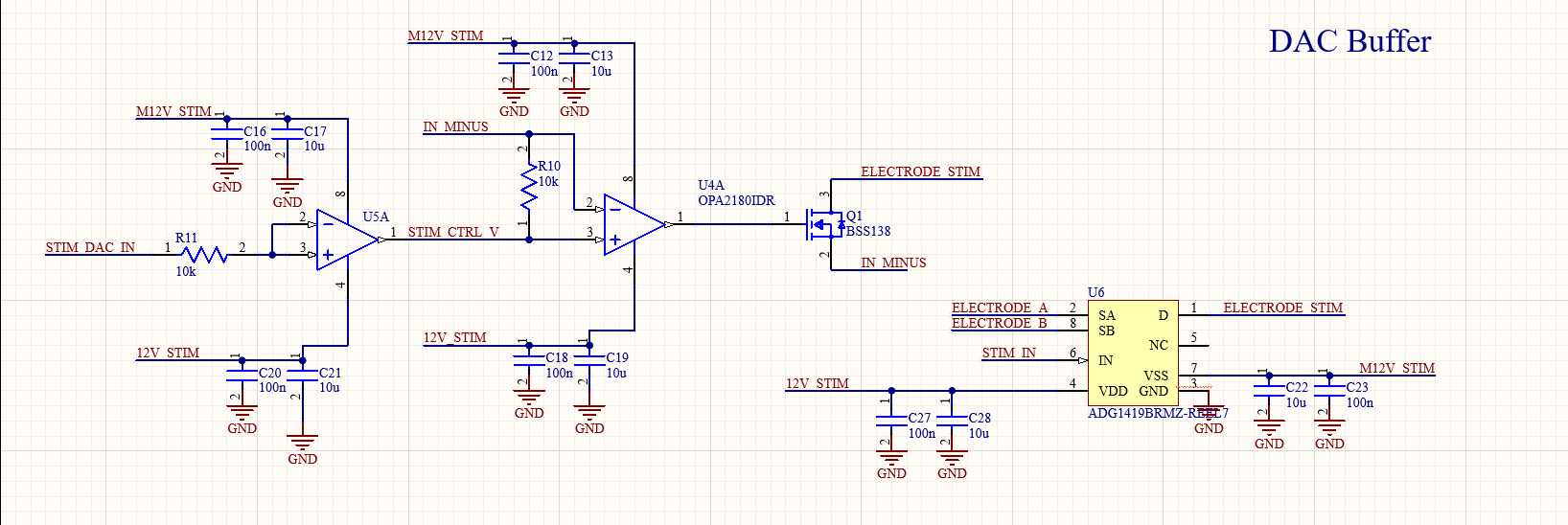
Instead of relying on analog switches for multiplexing auxiliary inputs, this system integrates a dual-channel, high-resolution AD5689R DAC paired with two OPA280 precision op-amps configured as unity-gain buffers. This design was implemented to support analog biasing, calibration signal injection, or programmable stimulation reference levels within the front-end signal path.
The AD5689R was selected for its:
- 16-bit resolution and ±2 LSB INL accuracy, providing sub-millivolt tuning precision
- SPI communication interface for low-noise digital control via the STM32
- On-chip 2.5V reference and dual outputs for compact power-constrained designs
- 0V–2.5V output range, ideal for unipolar control signals in analog front-ends
Because the DAC’s output has limited drive capability and exhibits non-negligible output impedance, I used OPA280 op-amps configured in a unity-gain buffer configuration. These op-amps were chosen for their:
- Low input offset voltage (50 μV typ) and low bias current (±0.5 nA), preventing distortion of reference signals
- Rail-to-rail input and output, maximizing dynamic range at low supply voltages
- Fast slew rate and high open-loop gain for clean transient response and accurate tracking
Each DAC output feeds directly into the non-inverting input of an OPA280, and the output of the op-amp drives downstream analog control paths, such as programmable voltage references for stimulation modules or active bias injection in amplifier circuits. This setup ensures that any digitally commanded voltage is faithfully reproduced at the output, independent of downstream load conditions or analog front-end impedance.
Compared to switch-based architectures, this DAC-buffer approach enables precise, programmable analog control across two independent channels, eliminates transient switching artifacts, and lays the groundwork for future closed-loop neurostimulation protocols with dynamic setpoints.
60 Hz Twin-T Notch Filter
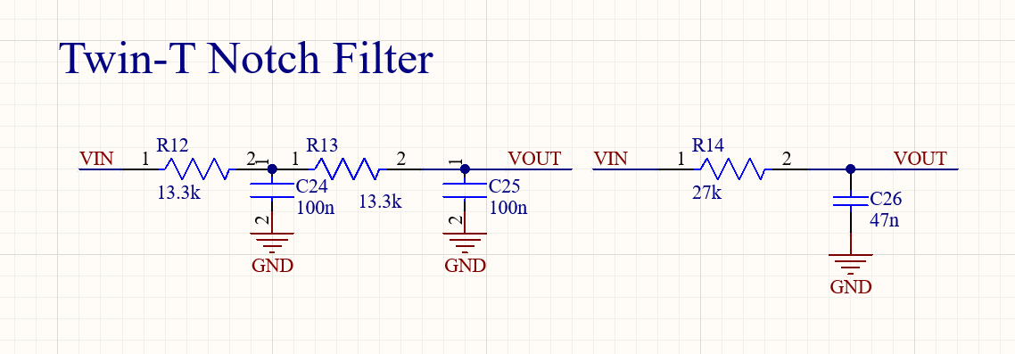
Mains noise was eliminated using a passive Twin-T Notch Filter. The filter is centered at 60 Hz using:
fnotch = 1 / (2πRC)
Using R1 = 13.3kΩ, R2 = 26.5kΩ, C1 = 100nF, and C2 = 47nF, I achieve a deep notch at 60 Hz. This was preferred over active or digital filtering due to its zero latency, no computation overhead, and phase-preserving characteristics—critical in preserving waveform fidelity for decoding.
Anti-Aliasing Low-Pass Filter

To suppress noise above the Nyquist frequency, a low-pass RC filter was placed downstream of the notch:
fc = 1 / (2πRC)
With R = 12kΩ and C = 0.1μF, the cutoff frequency was ~132 Hz. This helped reduce the aliasing of high-frequency power and RF noise while maintaining bandwidth for physiological signals (0.5–100 Hz range).
Analog-to-Digital Converter – ADS1118
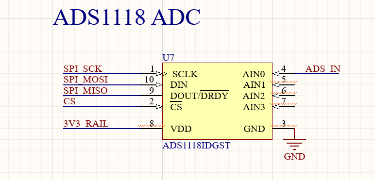
The ADS1118 was selected for its 16-bit resolution, SPI interface, and programmable gain amplifier. It provided high-resolution digitization with selectable full-scale input ranges, including ±2.048V—ideal for the INA333’s output. The integrated temperature sensor was also used to monitor ambient board temperature.
STM32F103C8T6 Microcontroller
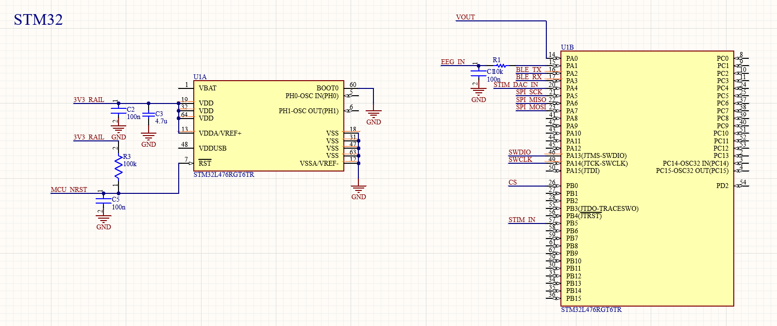
This MCU offers an ideal trade-off between power, performance, and cost. Its 72 MHz clock and low power modes allowed efficient sampling and logging, while its SPI and UART peripherals enabled flexible interfacing with sensors, ADC, microSD, and telemetry. Alternatives like the nRF52840 were considered but added complexity in BLE firmware which will be tackled in future iterations.
Power System Architecture
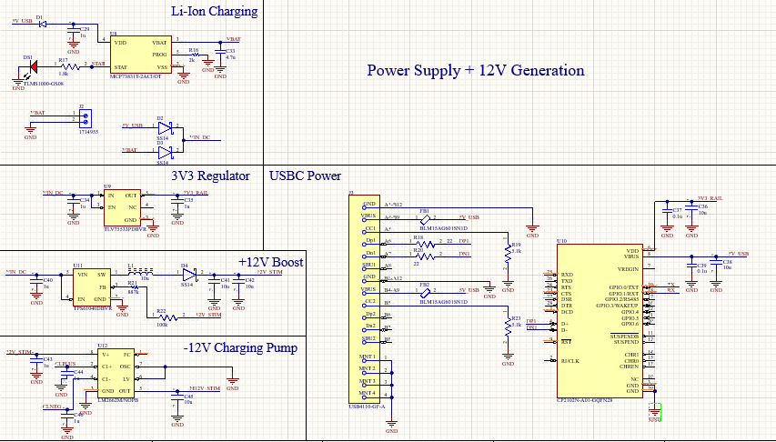
- USB-C Input: A protected USB-C port provides the primary 5V power rail. ESD diodes protect the downstream electronics.
- Li-Ion Charging: A TP4056 module allows safe charging of 3.7V Li-Ion batteries with built-in thermal protection and status LED indicators.
- 3.3V Regulation: The AMS1117-3.3 LDO provides regulated 3.3V for MCU and analog circuits. Its dropout and PSRR performance was suitable for biopotential systems.
- +12V Boost: A TPS6104 boost regulator provides a 12V rail from the 5V line for future use with stimulators or sensor biasing circuits.
- -12V Inversion: The LM2662M charge pump inverter generates a -12V rail, enabling bipolar stimulation or reference voltage generation for op-amps in future closed-loop circuits.
microSD + RTC Logging
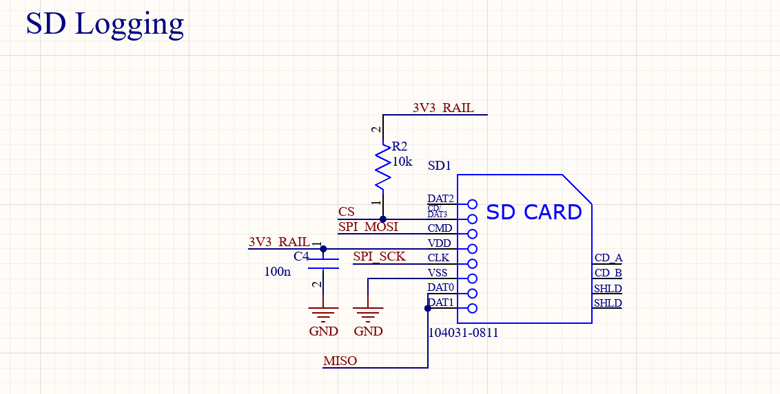
A DS3231 real-time clock and microSD card were integrated to allow reliable timestamped signal logging for hours or days without requiring a BLE or PC interface. This architecture allowed wearable use in field trials and lab studies without constant tethering.
Thermal Fault Protection
A voltage divider and NTC thermistor formed a comparator circuit to monitor temperature. The comparator (e.g., LM393) tripped a digital pin high if the sensed voltage crossed a threshold—indicating overheating. This triggered a hardware shutdown or warning, preventing patient or system damage.
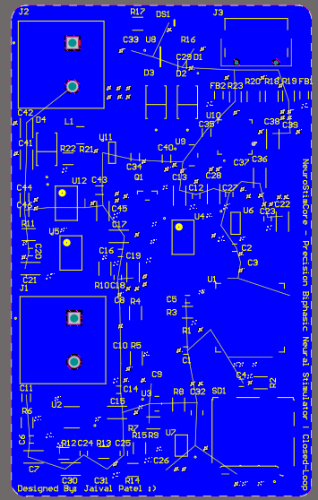
PCB Layout Strategy
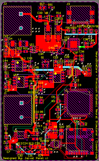
The Medical-Grade Sensor Node was implemented on a six-layer PCB, optimized for clean analog signal paths, robust digital communication, and modular power delivery. The stack-up is as follows:
- Top Layer: Mixed Power + Signal
- Layer 2: Analog Signal
- Layer 3: Dedicated Power Plane (split by domain)
- Layer 4: Digital Signal
- Layer 5: Analog Signal + DAC Routing
- Bottom Layer: Continuous Ground Plane
Analog vs. Digital Domain Separation
Analog and digital zones were carefully partitioned both physically and electrically. The ADC, instrumentation amplifier (INA333), DAC (AD5689R), and analog buffers (OPA280) were placed in the top-left corner of the board, isolated from high-frequency digital lines. Each analog component was referenced to a local analog ground island connected to the main ground plane via a single-point bridge near the ADC.
The STM32, microSD slot, and RTC were placed in the opposite quadrant to localize switching noise. Key digital lines (SPI, UART, I2C) were routed on Layer 4 and shielded by adjacent power and ground planes to reduce crosstalk into sensitive analog domains.
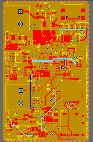
DAC Buffer Routing Considerations
The dual-channel DAC (AD5689R) and its OPA280 buffers required specialized routing on Layer 5. To minimize capacitive coupling and DC offset drift:
- Each DAC output trace was kept under 500 mils and routed directly into the non-inverting input of the OPA280
- Output traces from the op-amps were routed over continuous analog ground to suppress EMI pickup
- Guard rings were deployed around both DAC and op-amp outputs to isolate them from fast-switching signals
- Bypass capacitors (0.1 µF + 4.7 µF) were placed within 1 mm of both DAC and op-amp supply pins
Instrumentation Amplifier Signal Integrity
The INA333's differential inputs were routed as tightly coupled traces with matched lengths (less than 10 mil difference) and minimal vias. Each trace passed through a 10 kΩ + 10 nF low-pass filter near the connector, followed by ESD protection diodes before reaching the amplifier. The output of the amplifier was routed into both the Twin-T notch filter and then the anti-aliasing filter, using Layer 2 (analog signal) to avoid interference.
Power Distribution and Isolation Strategy
Each power domain (+3.3V logic, +12V boost, -12V inverter, USB input) was separated using ferrite beads with high impedance at 1 MHz. The TPS6104 boost converter and LM2662 charge-pump were placed near the edge of the board to reduce thermal coupling into sensitive analog areas.
Via stitching was used across ground and power pours to reduce loop inductance, especially around power input connectors, the DAC subsystem, and the ADS1118 ADC. All regulators had dedicated ground returns routed directly to the bottom GND plane as seen in Figure 11.
Signal Routing and Clock Domains
SPI lines for the ADS1118 and AD5689R were grouped and routed as impedance-controlled pairs on Layer 4. Pull-up and termination resistors were placed close to the MCU. The system clock from the STM32 was kept away from analog zones to avoid radiated noise coupling into the EEG front-end.
Thermal and Mechanical Layout Considerations
All voltage regulators and analog buffers were given generous copper pour heatsinking on the top and power layers. Thermal relief vias were added underneath the AMS1117 and TPS6104 packages to distribute heat across layers. Mounting holes were isolated with clearance rings and tied to system GND for ESD protection.
Connector Placement and Access
The USB-C, SD card, and battery connectors were placed along the same edge to facilitate enclosure design and cable routing. The EEG input connector was shielded by copper ground fences and placed on the opposite edge to minimize mechanical noise coupling into signal traces.
All analog traces remained below 6 inches in length, had minimal stub loading, and were verified for parasitic coupling using Altium’s signal integrity analyzer.
Testability and Debug Infrastructure
Test points were added for DAC outputs, analog bias lines, comparator fault flags, and each power rail. The DAC outputs, in particular, were routed to accessible headers for oscilloscope probing, allowing real-time validation of signal integrity and tracking behavior of the buffered analog control signals.
Challenges & Future Work
- Minimizing thermal hotspots near LDOs in small enclosure
- Managing analog-digital crosstalk on tightly packed board
- Fine-tuning threshold voltage for thermal trip logic under dynamic load
- Next Steps: BLE streaming, embedded neural decoding inference, miniaturized wearable form factor
Tools & Skills Used
- Altium Designer – Schematic capture and multilayer PCB layout
- STM32CubeIDE – Embedded firmware (ADC control, SPI, RTC, logging)
- MATLAB – Filter design and transfer function analysis
- Bench Debugging – Oscilloscope, logic analyzer, thermal camera
- Power Budgeting – Sleep-mode profiling, runtime simulations