Neural AFE
Overview
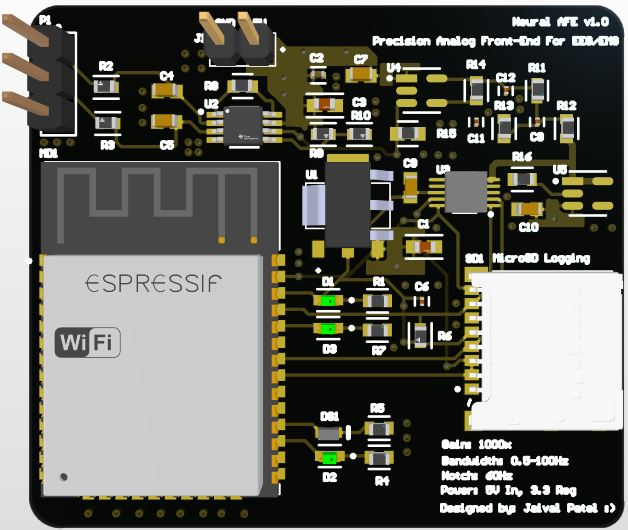
The Neural AFE Board is a precision analog front-end platform designed to acquire low-amplitude biopotential signals (e.g., EEG, EMG) in electrically noisy environments. The system integrates ultra-low noise amplification, 60 Hz notch filtering, hardware-level protection, and STM32-based data acquisition. Designed on a 4-layer PCB, the board targets automotive-grade and neurotech applications for real-time signal analysis and edge AI integration.
Key Features
Instrumentation Amplifier: INA333
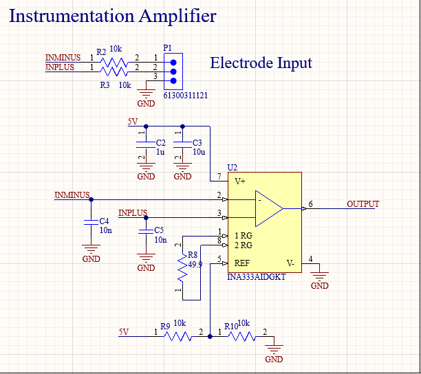
The INA333 was selected for its low input bias current (200 pA typ), low offset voltage (25 µV typ), and ultra-low quiescent current (50 µA typ). The gain was set to approximately 1000 using the following formula:
G = 1 + (50kΩ / RG)
Solving for RG = 49.9Ω, we achieve:
G ≈ 1 + (50,000 / 49.9) ≈ 1002
This configuration offers high gain with minimal external components, ideal for microvolt-level signal extraction with minimal noise contribution.
Input Protection and Filtering
A 10 kΩ resistor in series with a 10 nF capacitor forms a low-pass RC filter:
fc = 1 / (2πRC) = 1 / (2π * 10kΩ * 10nF) ≈ 1.59 kHz
This suppresses high-frequency noise while offering negligible signal distortion in the 0–100 Hz EEG band.
Reference Voltage Divider and Buffering
A mid-supply reference is created using two 10kΩ resistors and a 1 µF capacitor:
VREF = VCC / 2 = 3.3V / 2 = 1.65V
This reference is buffered using a MCP600 op-amp in unity-gain configuration to reduce impedance and stabilize biasing.
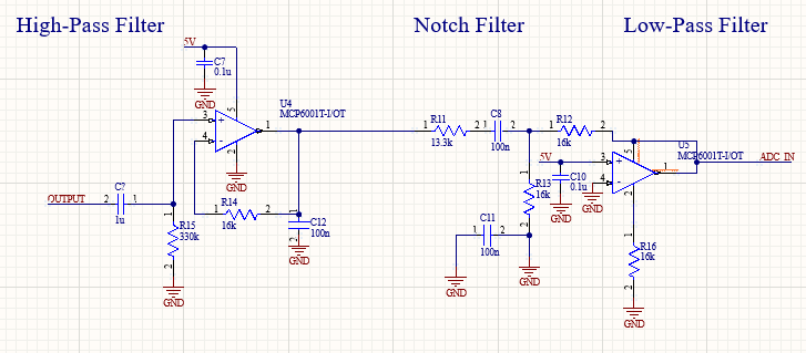
High-Pass Filtering for DC Rejection
A series capacitor (1 µF) and a 330 kΩ resistor form a high-pass filter:
fc = 1 / (2πRC) ≈ 0.48 Hz
This removes slow DC drift while preserving all meaningful neural activity in the frequency band of interest. See Figure 3 for more information.
Notch Filter for Power Line Rejection
A twin-T notch filter was designed using the following component values: R1 = 13.3 kΩ, R2 = 26.5 kΩ, C1 = 47 nF, C2 = 100 nF
The notch frequency is determined by:
fnotch = 1 / (2πRC) ≈ 60 Hz
This configuration yields strong attenuation at 60 Hz, eliminating power-line interference in indoor environments. See Figure 3 for more information.
Microcontroller: STM32F103C8T6
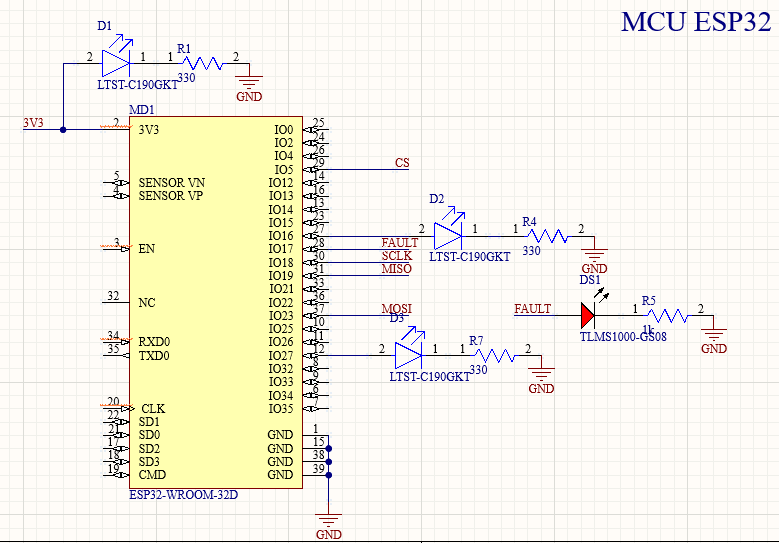
Selected for its cost-effectiveness, built-in ADCs, and broad software support. UART and USB support allows seamless integration with downstream logging or edge ML systems. Analog inputs are buffered to reduce noise coupling.
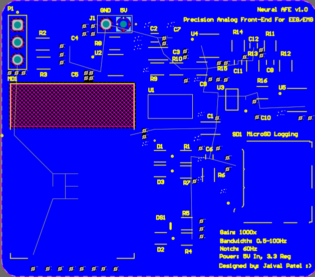
PCB Layout Strategy
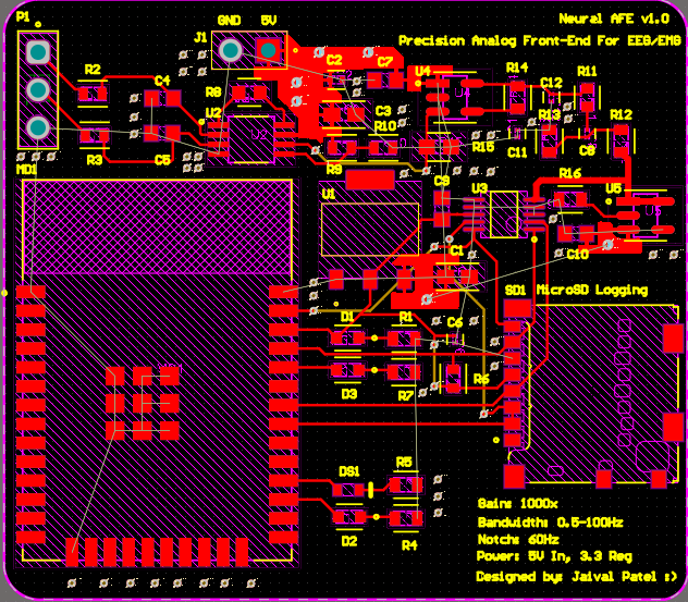
The board uses a 4-layer stackup: Top Layer (Components + Power), Layer 2 (Signal), Layer 3 (Power), Bottom Layer (GND). Key layout decisions include:
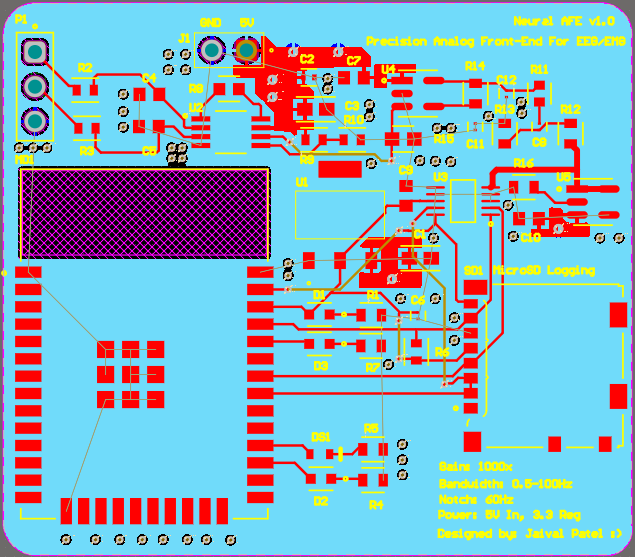
- Component Grouping: Analog front-end kept isolated from STM32 and USB sections.
- Ground Stitching: Star-ground topology maintained between analog and digital domains.
- Via Strategy: Short thermal vias placed under op-amps and voltage divider to stabilize heat.
- Signal Integrity: Filter caps placed as close as possible to power and signal pins; differential pairs routed for USB lines.
- Routing Discipline: No traces cross the notch filter layout to avoid loop interference.
Challenges & Constraints
- Achieving high gain (1000×) without saturating due to input offsets or bias leakage.
- Maintaining analog signal fidelity while sharing power/ground with digital logic (STM32).
- USB-C routing required tight impedance control and precise matching to USB 2.0 spec.
- Thermal isolation was necessary for stable reference voltage generation under varying load.
- Board space was limited to a handheld form factor, requiring high-density routing and compact component selection.
Tools Used
- Altium Designer: Schematic + multi-layer PCB design
- LTspice: Twin-T and high-pass filter simulation
- STM32CubeIDE: Embedded firmware development and serial data transmission