HIL-Testing Rig
The HIL (Hardware-in-the-Loop) Testing Rig is a custom-designed emulation board aimed at accelerating embedded system validation and debugging for safety-critical applications. The rig enables real-time injection of analog/digital faults, emulation of sensor input/output via DAC and ADC components, high-throughput logging via SPI Flash, and telemetry through USB and CAN interfaces. It is built around the STM32F103C8T6 microcontroller and designed with a modular 6-layer stackup to isolate analog, power, and digital zones. The system supports rapid iteration cycles for embedded firmware by simulating real-world scenarios through precisely controlled test signals.
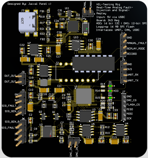
Key Features
The HIL Testing Rig was designed from first principles to simulate sensor, actuator, and fault conditions that embedded systems experience in real-time deployments. The following subsystems were added with careful consideration for functional fidelity, hardware test coverage, and compatibility with industry debugging tools.
DAC + ADC Emulation I/O
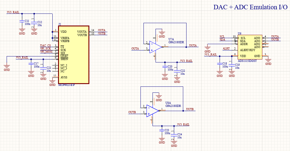
I included dual 12-bit DACs (MCP4922) and 16-bit ADCs (ADS1118) to simulate real-world analog input and output lines. The DACs drive test voltages into target MCU pins while the ADCs measure back-sensed voltages and responses. These components were selected for:
- SPI communication for noise-isolated digital control
- Voltage reference tunability for diverse signal conditions
- Proven compatibility with STM32 systems
The DACs were buffered using dual-OPA280 op-amps to ensure consistent drive capability under varying load impedances. This guarantees accurate test voltage sourcing without droop or overshoot.
Fault Injection Subsystem
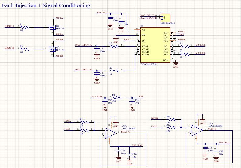
Fault injection logic was implemented using DIP switch arrays and analog switches (TS3A5018) to selectively short lines, introduce open conditions, or force stuck-at values. This design supports testing against edge-case scenarios such as:
- Short to VDD/GND
- Signal oscillation or brownout simulation
- Forced transitions to validate firmware debounce and recovery
Power Management
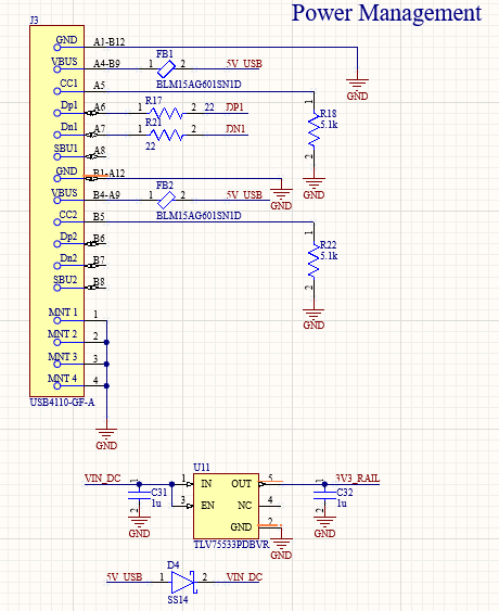
The board accepts a 12V external input through a Molex Micro-Fit connector. A LDO (TLV7553) steps this down to 5V and 3.3V rails. Decoupling capacitors and ferrite beads isolate the analog and digital planes. This ensured:
- Low ripple supplies for analog front-end devices
- Stable core voltage for STM32 operations
- Expandable rails for future high-current simulation peripherals
SPI Flash Logging
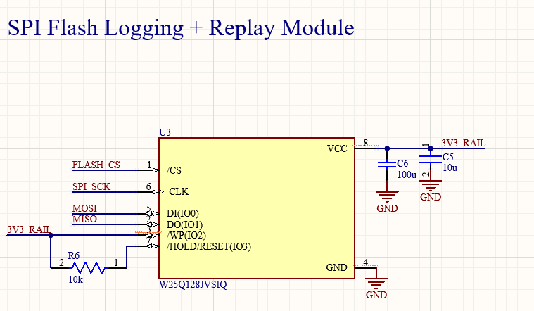
An external 8MB SPI Flash (W25Q64JV) was included for logging waveform, event timing, or system responses during test runs. Chosen for its high throughput and endurance, this allows for offline inspection of:
- ADC response to fault injection
- Voltage rail behavior during load shifts
- Digital toggle patterns and control signal performance
Firmware logs data at configurable sampling rates and tags with event timestamps from a 32.768kHz-driven RTC.
STM32F103C8T6 Microcontroller
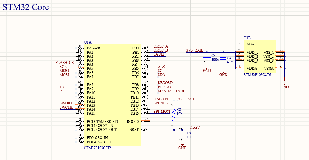
The core controller was chosen for its mature development ecosystem and peripheral availability:
- SPI buses for DAC/ADC/Flash
- USART + CAN interface
- DMA and timer channels for low-latency tasks
Test Headers
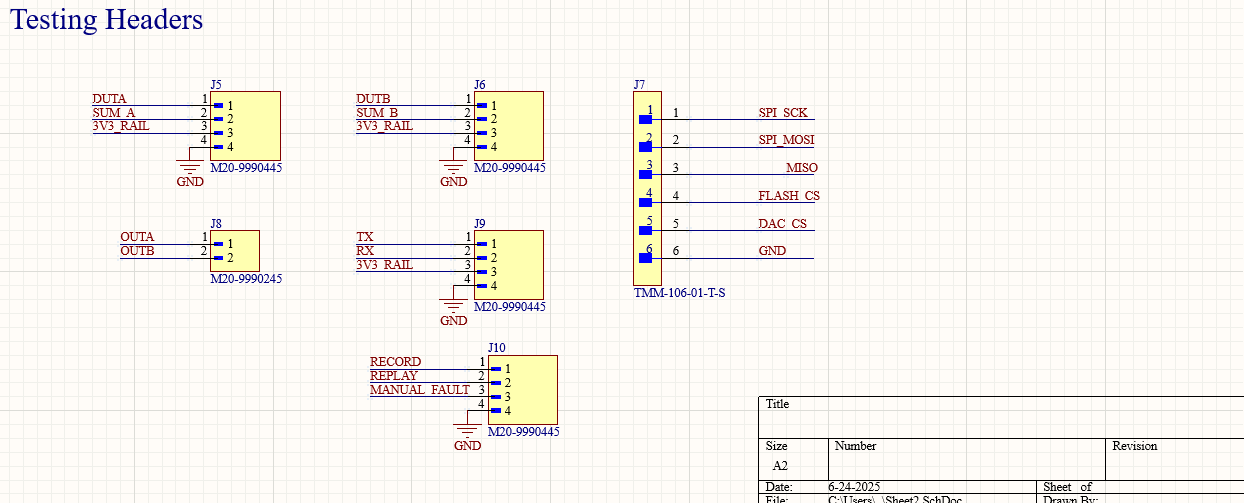
All internal signals—fault injection lines, DAC output, ADC input, and SPI interfaces—were routed to labeled 0.1" headers. This enabled quick:
- Oscilloscope probing for validation
- Re-routing during board bring-up
- Patch wire debugging during firmware development
USB + CAN Telemetry System
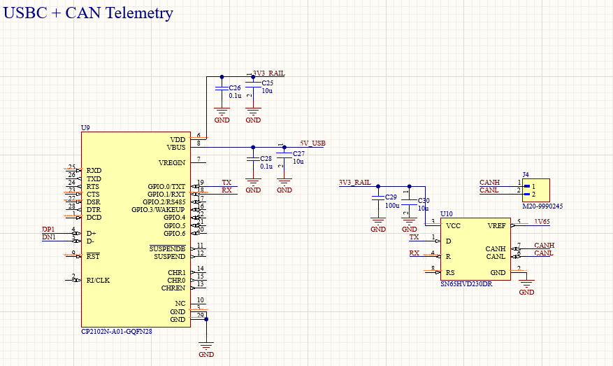
To interface with host PCs or test control platforms, the board included:
- USB-C connector with onboard ESD protection
- SN65HVD230 CAN transceiver for real-time telemetry injection
USB was used for log retrieval and test initiation, while CAN enabled streaming status and triggering commands within larger HIL simulation clusters.
System Boot & Initialization
- 1. Clock Configuration: Set system clock to 72 MHz using PLL from internal 8 MHz RC.
- 2. GPIO Initialization: Configure:
- - Analog switch control pins (PB0-PB4) as outputs
- - Mode switches (PB10-PB12) as inputs with pull-downs
- - LEDs (PC13 - PC15) as outputs
- 3. SPI Initialization: SPI1 initialized for full-duplex mode at 8 MHz
- 4. I2C Initialization: I2C1 initialized at 400 KHz (Fast Mode)
- 5. UART Initialization: UART1 configured at 115200 baud
- 6. ADC & DAC Emulation Setup: Dummy values preloaded into DAC buffer
- 7. Flash Check: Verify W25Q128JV is responsive and ready for logging
Fault Injection Logic
Control Pins
- PB0: Dropout Enable (TS3A5018 CH1)
- PB1: 3V3 Spike Inject (CH2)
- PB2: GND Inject (CH3)
- PB3: DC Offset Toggle (CH4)
- PB4: Noise Mode Enable (DAC_B replay)
- GPIOs controlled via custom-writte-function in firmware
- In Replay Mode, faults are injected at fixed intervals (or toggled by switch PB12)
- In Capture Mode, faults can be manually activated for DUT stress testing
Logic
PCB Layout Strategy & Challenges
The HIL Testing Rig was laid out on a 6-layer PCB stackup to accommodate its dense analog-digital subsystems while maintaining signal integrity and power stability. The stackup was as follows:
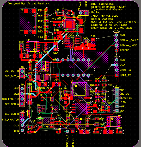
- Top Layer: Power + Signal (mixed analog and SPI)
- Layer 2: Ground (solid reference plane)
- Layer 3: Power (filtered rails: 3.3V, 5V)
- Layer 4: Digital Signals (MCU to flash, DAC/ADC)
- Layer 5: Shield + control signal stubs
- Bottom Layer: Ground with test-point silkscreen access
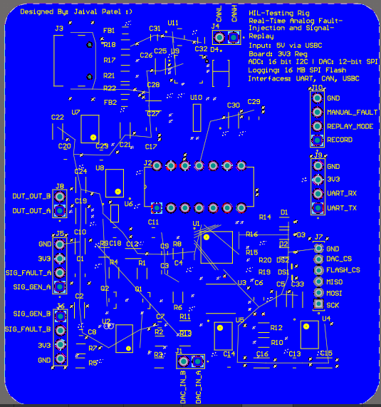
Power was partitioned into separate islands for the analog front end (DAC/ADC/buffers), the MCU core logic, and the fault simulation logic. This minimized coupling between noisy switching traces and sensitive voltage sources. Decoupling was handled by placing high-frequency 0.1μF capacitors near every VDD pin and 10μF bulk capacitors per rail per zone.
CAN signals were routed on Layer 2 with matched impedance, using short stubs and differential trace pairs. Fault injection switches were centrally located, allowing short, symmetric routes to each simulated net. The DAC/ADC traces were routed over continuous ground and passed through low-pass filtering stages before test access.
Large copper pours were used to aid thermal dissipation, especially near the TPS54202 and polyfuse areas. SPI signal integrity was protected by series resistors and grounded shielding layers above and below Layer 4 traces.

Design Challenges
- Mixed-signal routing: Care was needed to prevent digital toggling from polluting DAC paths. I used copper ground shielding fences and perpendicular trace orientation between SPI and analog routes.
- Fault timing determinism: DIP switches were prone to bounce, requiring edge-stabilization logic and Schmitt triggers to provide clean transitions for repeatable tests.
- Thermal performance: The +12V power section initially exhibited excessive regulator heating; thermal reliefs and thicker traces were added to mitigate this.
- Analog output accuracy: DAC output impedance under load necessitated op-amp buffering (OPA280) to maintain linearity under dynamic conditions.
Future Work
- Move from DIP/manual fault control to microcontroller-controlled analog switches for automated fault sequencing.
- Upgrade to higher-resolution DACs and ADCs (e.g., 16-bit+) for biomedical and aerospace-grade sensor simulations.
- Add real-time waveform streaming and programmable profiles via onboard storage and UART/USB/CAN control APIs.
- Integrate touchscreen or GUI-based host dashboard for easier scenario control and telemetry visualization.