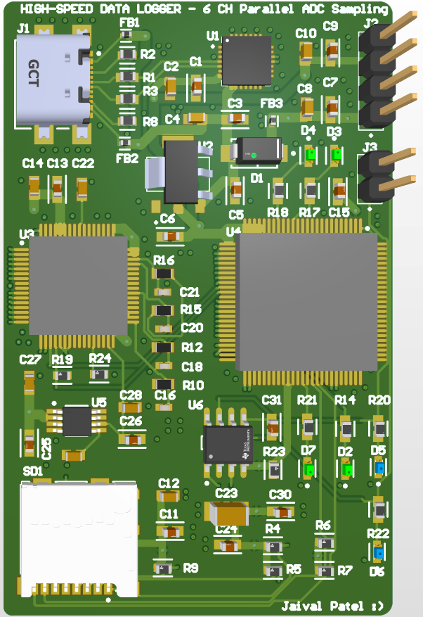
High Speed Data Logger - 6 Channel Parallel ADC Sampling
Overview
The High-Speed Data Logger is a purpose-built embedded system engineered to acquire, process, and log high-throughput analog sensor signals for advanced diagnostic and telemetry applications. Designed around the STM32F407VET6 microcontroller and six channels of simultaneous sampling using the ADS8556 ADCs, the system achieves real-time, multi-channel acquisition at up to 750 kSPS per channel, optimized for use cases ranging from robotics and vehicle diagnostics to neurotechnology signal capture.
To handle the resulting data throughput, the board uses SDIO-based microSD logging, supported by DMA buffers to eliminate CPU blocking. The design prioritizes low-latency data capture while maintaining analog integrity through careful PCB partitioning, power isolation, and signal conditioning. In addition to analog inputs, the board features a CAN interface for system telemetry, and a modular interface for optional sensor expansion.
The logger features a 6-layer mixed-signal PCB stackup, engineered for high-speed digital traces and low-noise analog performance. With onboard power management and ESD protection, it supports both field and lab testing environments, enabling engineers to stream, store, or post-process high-resolution waveform data with sub-millisecond fidelity.
This project showcases high-performance embedded architecture and system-level optimization, suitable for applications in automotive debugging, industrial instrumentation, and brain-computer interface research where data rate, precision, and logging robustness are mission-critical.
Key Features & Design Decisions
The High-Speed Data Logger project was developed to address a critical bottleneck in embedded data acquisition: the ability to sample, digitize, and log multiple analog channels in parallel at high resolution and speed. This is especially relevant for neurotechnology, motor control diagnostics, and sensor-rich applications where sub-millisecond signal events must be captured with fidelity. Each design decision—from part selection to architecture partitioning—was made with performance, noise resilience, and I/O concurrency in mind.
Parallel ADC Architecture (ADS8556)
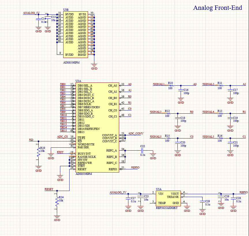
The core analog front-end consists of up to four Texas Instruments ADS8556 ADCs, each offering 6 channels of simultaneous sampling at 16 bits and up to 650 kSPS per channel. These devices were selected specifically for their:
- Parallel bus interface, enabling ultra-fast reads compared to serial SPI ADCs
- Simultaneous sampling architecture, which avoids inter-channel skew critical in applications like EEG or motor phase current logging
- Software-selectable gain ranges (+/-10V, +/-5V, etc.), making it ideal for mixed-voltage analog environments
Each ADS8556 was given a dedicated parallel bus mapped to STM32 GPIO ports, ensuring non-multiplexed communication and allowing true concurrent channel sampling and buffering.
Microcontroller Selection – STM32F407VET6
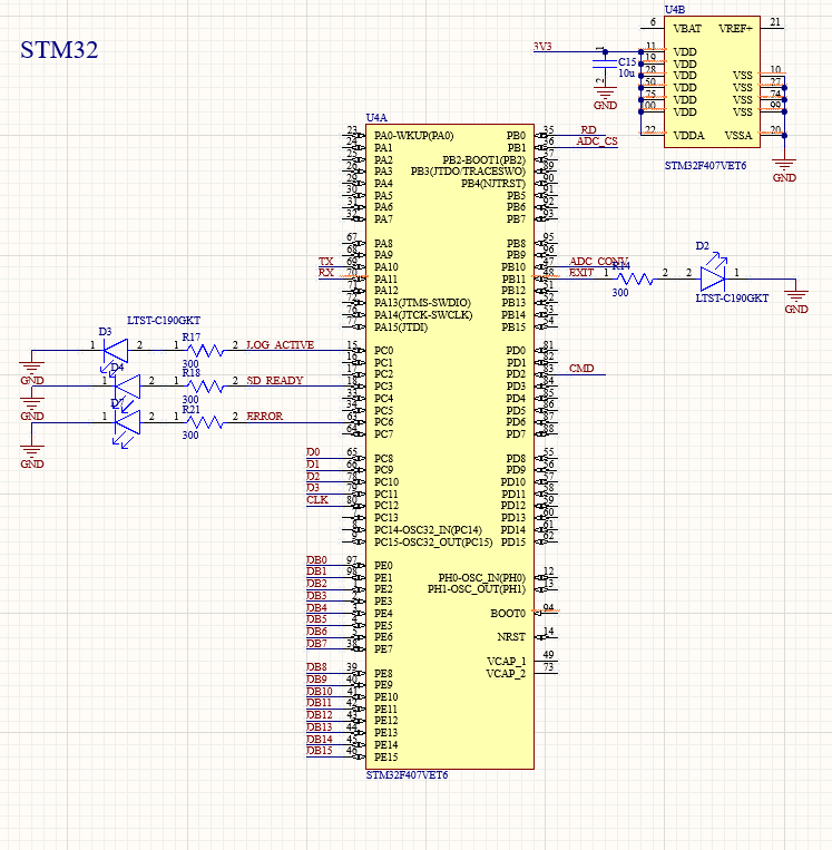
The STM32F407 was chosen over other Cortex-M3 and M4 series for several reasons:
- 168 MHz core clock with DMA support on GPIO and SDIO
- Rich memory footprint (512 KB Flash, 192 KB RAM) for buffering large ADC frames before writes
- SDIO interface for high-speed microSD writes up to 25 MB/s
- Multiple GPIO ports and external interrupt lines to interface with parallel ADCs and handle READY signals
Its STM32Cube ecosystem and RTOS integration also supported rapid development and deterministic task scheduling during data logging.
SDIO-Based microSD Logging
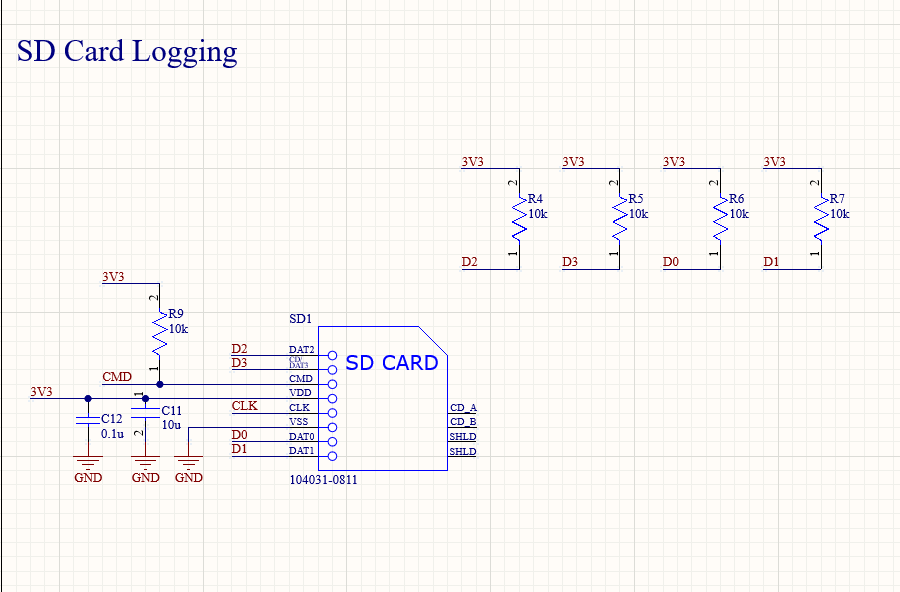
Logging performance was a top priority. The microcontroller's dedicated SDIO peripheral allowed high-speed writes to microSD cards using native 4-bit mode. This was crucial to sustaining >1 MSPS aggregate throughput across multiple ADCs. DMA was used to buffer and stream ADC frames in bursts, reducing CPU overhead and increasing bus efficiency.
CAN Telemetry and Debug Interface
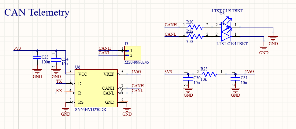
A SN65HVD230 CAN transceiver was integrated for telemetry and remote command injection during logging sessions. Unlike UART, which is susceptible to noise and limited in speed, CAN offers:
- Robust differential signaling for noisy environments
- Hardware filtering and packet arbitration
- High-speed mode (1 Mbps) when RS pin is tied to GND
This made the system compatible with robotics and automotive setups requiring synchronous status updates during acquisition.
Status LEDs and Visual Debug
The system includes multiple status LEDs to indicate:
- MicroSD detection and logging activity
- ADC synchronization errors
- Power sequencing status
This allowed real-time visual inspection during lab testing without external instrumentation.
Power Architecture and Regulation
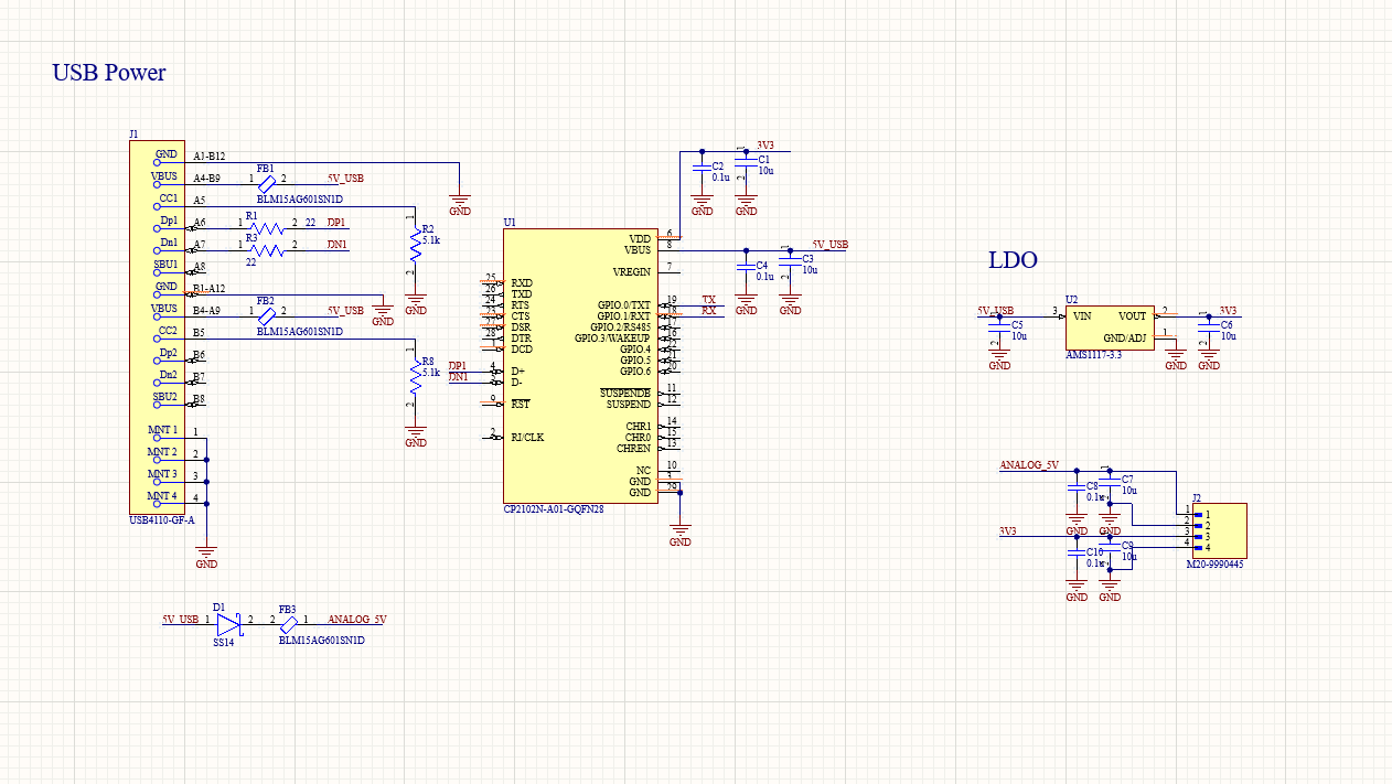
The board was designed to support either USB-C. Key regulators include:
- AMS1117-3.3V – powers STM32 and digital logic, chosen for availability and thermal performance
- Dedicated analog regulator (low-noise LDO) to feed the ADS8556 VREF and analog front-end, reducing digital cross-talk
Ground planes were split between analog and digital domains to isolate switching noise, and ferrite beads were used at domain transitions to suppress high-frequency ripple.
Header Configuration and Signal Routing
Each analog channel from the ADS8556 was routed through a header or jumper, allowing selective channel enabling, fault injection, or signal rerouting for debugging. These headers doubled as convenient scope probing points for confirming signal shape and timing at each acquisition stage.
EMC and Noise-Reduction Techniques
Analog input lines were protected with RC low-pass filters (e.g., 10kΩ + 100pF) at each input pin to reduce aliasing and ESD. Digital traces were kept short and routed over uninterrupted ground planes to minimize loop area and coupling. Careful layout separation ensured the microSD and CAN domains did not radiate into ADC lines.
Design Scalability
Although initially tested with two ADCs, the board supports up to four parallel ADS8556 devices. This flexibility was designed in from the start, with:
- Extra GPIO expansion via STM32 alternate pin-mapping
- Dedicated headers for extra ADC VIN lines
- Selectable VREF circuitry for varying voltage domains
This design foresight makes the system extensible to future use cases like multi-sensor fusion, high-speed tactile input recording, or dense motor current analysis.
PCB Layout Strategy
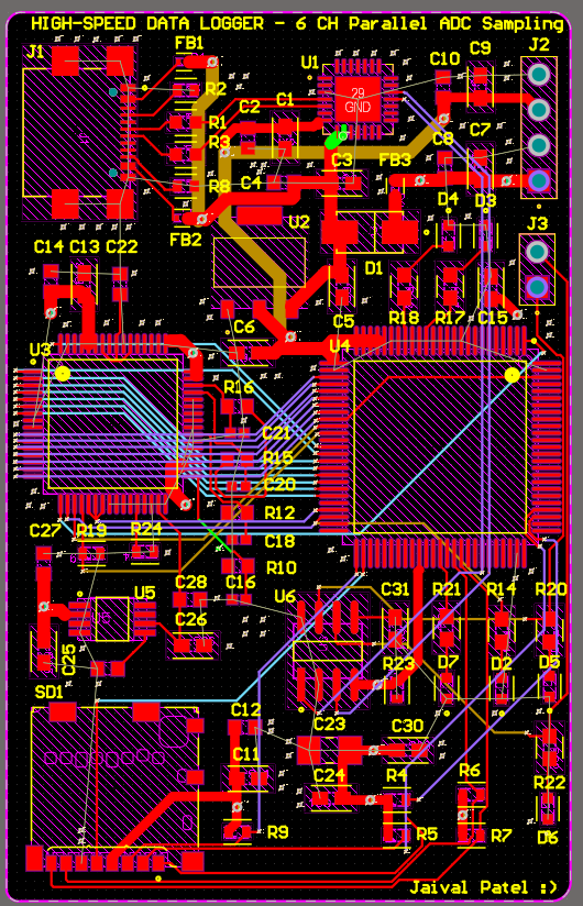
The High-Speed Data Logger was architected with layout precision as a top priority to accommodate high-throughput analog data capture without compromising signal integrity, thermal stability, or electromagnetic compliance. The board utilizes a dense 6-layer stackup with a well-partitioned routing strategy to isolate noisy digital interfaces from sensitive analog input traces, while ensuring optimal power delivery to high-speed devices.
Layer Stackup Rationale
The board features the following 6-layer structure:
- Top Layer: Power + Signal (Component Placement)
- Layer 2: 3.3V Dedicated Power Plane
- Layer 3: Analog Front-End Signal
- Layer 4: Digital Signal Routing
- Layer 5: Internal Signal + Control Power
- Bottom Layer: Solid GND Plane
Analog Front-End Layout
The ADS8556 ADCs—key to our high-speed acquisition—were placed with direct proximity to their corresponding analog input headers and decoupling capacitors. Input traces were routed as tightly-coupled differential pairs with controlled impedance, avoiding any layer transitions that could introduce reflections or parasitics. Key considerations included:
- Guard rings around high-impedance analog nodes to prevent leakage
- Dedicated analog GND pour zones electrically connected to the main GND only at a single star point
- Matched trace lengths for simultaneous sampling across channels
Digital Domain Partitioning
All high-speed SPI lines, microSD SDIO lines, and STM32 GPIO traces were isolated to digital-only zones. These were routed predominantly on Layers 4 and 5, with impedance-controlled traces and series resistors where signal integrity analysis indicated potential for overshoot. The STM32F407VET6 microcontroller was centered between the analog front-end and logging subsystems to minimize signal delays and fan-out routing.
High-Speed Logging Interface
The SDIO-based microSD interface was prioritized for signal integrity by:
- Using impedance-matched traces (45–50Ω single-ended) for CLK, CMD, and D0–D3
- Adding a local ground reference pour under the SDIO interface to prevent reflection and cross-coupling
- Routing short, direct traces to avoid stubs and uncontrolled impedance
Power Delivery Network (PDN)
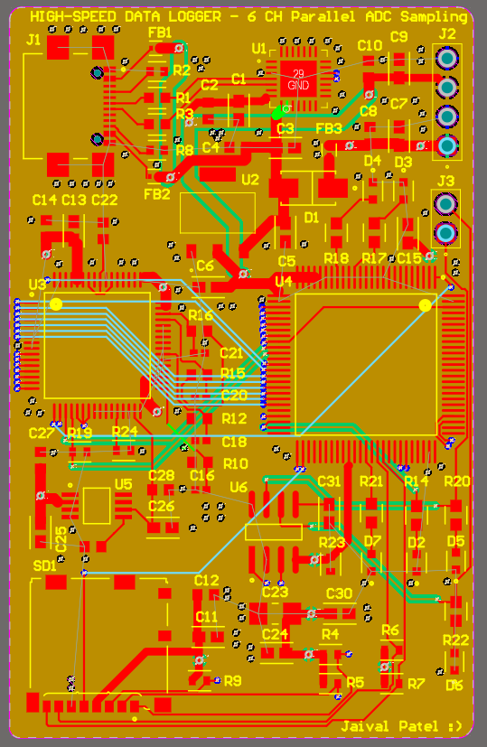
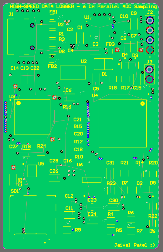
The 3.3V plane was sandwiched between ground and signal layers to minimize power loop inductance. Each active device (ADC, MCU, microSD) received local ceramic decoupling (100nF + 1µF) positioned within 1 mm of VDD pins. Bulk electrolytics supported low-frequency transients, especially for the SD card current surges during burst writes.
CAN Telemetry Zone
The SN65HVD230 CAN transceiver was placed near the board edge, with differential traces for CAN_H and CAN_L routed as a tightly coupled pair with 120Ω termination. These lines were kept away from the analog front-end and routed over a consistent ground reference plane to preserve the differential impedance and reduce susceptibility to common-mode noise.
Clock & Control Signals
Crystal oscillators for the STM32 and any auxiliary timing circuitry were placed as close as possible to their associated ICs, with symmetric guard traces and ground pour to shield from adjacent signal lines. Oscillator load caps were matched to minimize startup skew, and stubs were avoided on clock lines.
Thermal Management
While power dissipation was low, the STM32 and ADCs can generate moderate localized heat during burst logging. Copper pours beneath high-power ICs were thermally stitched using vias to inner and bottom layers to spread heat. Sensitive analog sections were kept thermally decoupled by layout zoning.
Silkscreen & Debug Accessibility
All debug headers were labeled clearly with orientation dots and functional markings (e.g., “ADC IN 1–6”, “CAN TX/RX”, “SDIO CLK”). GPIO test pads were exposed with clearance around them for easy clip-on access with oscilloscope probes during firmware validation. Mounting holes were placed symmetrically for enclosure compatibility.
Design Rule Strategy
Critical trace width, clearance, and via rules included:
- 20 mil power traces for MCU and ADC core VDD
- 12 mil differential pair width and spacing for CAN lines
- 10 mil standard signal routing width
- 20 mil clearance between analog and digital zones
- Thermal reliefs for all regulator output pads
Challenges & Future Work
Design-Time Challenges
One of the foremost challenges was balancing high-speed digital logging with low-noise analog acquisition on a single board. The data logger needed to support simultaneous sampling across six ADC channels while writing to an SD card via SDIO at speeds upwards of 8–10 Mbps. This created three significant design bottlenecks:
- Signal Integrity: Digital switching noise from the SDIO interface risked coupling into the analog front-end. Careful layer partitioning and dedicated power planes were required to isolate domains and preserve measurement accuracy.
- Power Supply Stability: The SD card’s burst current demand often exceeds 100 mA, which can cause brownouts or ripple on the 3.3V line. This was mitigated using aggressive decoupling (both ceramic and bulk capacitors), ferrite isolation, and via stitching to distribute return paths.
- Trace Routing Complexity: With six analog channels, a microcontroller, high-speed SPI interfaces, and CAN transceiver all needing direct, clean routing, congestion was inevitable. The 6-layer stackup allowed sufficient flexibility, but forced a strict hierarchy of layer usage: analog signals and ground routing were locked early to avoid cross-domain interference.
Firmware Bottlenecks
Although the STM32F407 provides a powerful Cortex-M4 core and DMA engine, tuning DMA for high-throughput SDIO logging under real-time constraints was non-trivial:
- DMA transfer completion interrupts had to be processed without stalling ADC sampling loops.
- Buffer overruns during long SD card write bursts necessitated a ring-buffer scheme in SRAM, which consumed nearly 70% of the available 192KB RAM.
- Clock synchronization between ADC sampling, SPI reads, and SDIO transfers required both hardware timers and software-controlled flow management to avoid race conditions.
ADC Channel Crosstalk & Noise
During testing, small artifacts were noticed on adjacent ADC channels when high-frequency signals were injected on a single input. These appeared to be caused by:
- Shared ground return paths between ADC input pins
- Capacitive coupling on long analog traces adjacent to digital SPI lines
- Insufficient shielding for high-impedance ADC inputs
CAN Debugging Latency
The SN65HVD230 CAN transceiver was added to enable system-level integration and logging into broader diagnostic platforms. However, under high traffic conditions, collisions and bit-stuffing created delays in transmission. A hardware workaround involved using the STM32’s CAN FIFO and time-triggered transmission scheduling to reduce latency jitter and improve CAN throughput consistency.
Future Improvements
- Upgrade to Parallel Flash: Replacing the SD card with QSPI flash (e.g., Winbond W25Q256) would allow faster, deterministic logging without file system overhead.
- Onboard ML Inference: Integration of a lightweight CNN or SVM model using CMSIS-NN to classify signals (e.g., neural spike detection) in real time.
- BLE Telemetry Stack: Adding a BLE module (e.g., nRF52 or ESP32) would allow real-time wireless preview of high-priority data, ideal for wearable or implantable research scenarios.
- Shielded Analog Daughterboard: Moving the analog front-end onto a shielded daughterboard would further isolate noise and permit easy replacement or upgrades to the signal chain (e.g., different filters or gain stages).
- Streaming Over USB-C: USB CDC logging could supplement or replace microSD-based logging for continuous desktop-based debugging environments.