Smart Electromechanical Testing Rig
Overview
The Smart Electromechanical Testing Rig is a custom-designed embedded system used to monitor, log, and visualize mechanical and electrical parameters during actuation, load-bearing, or response testing. Designed around the ESP32 for its wireless capabilities and low-power operation, the board integrates current sensing, voltage monitoring, visual feedback, and onboard data logging to enable both automated and hands-on testing workflows.
Traditional test rigs require bulky DAQ systems or rely on expensive industrial platforms. For academic and rapid prototyping settings, there’s a clear need for a low-cost, compact, and wireless-capable system that can interface with sensors, log data locally, and communicate with host systems or dashboards. This project bridges that gap, offering modular test instrumentation in a field-ready form factor.
Key Features & Design Decisions
The Smart Electromechanical Testing Rig was developed with the vision of providing a modular, reliable, and extensible platform for embedded diagnostics, test automation, and field measurements. Every component decision reflects a balance of technical merit, cost efficiency, low-power operation, and integration simplicity.
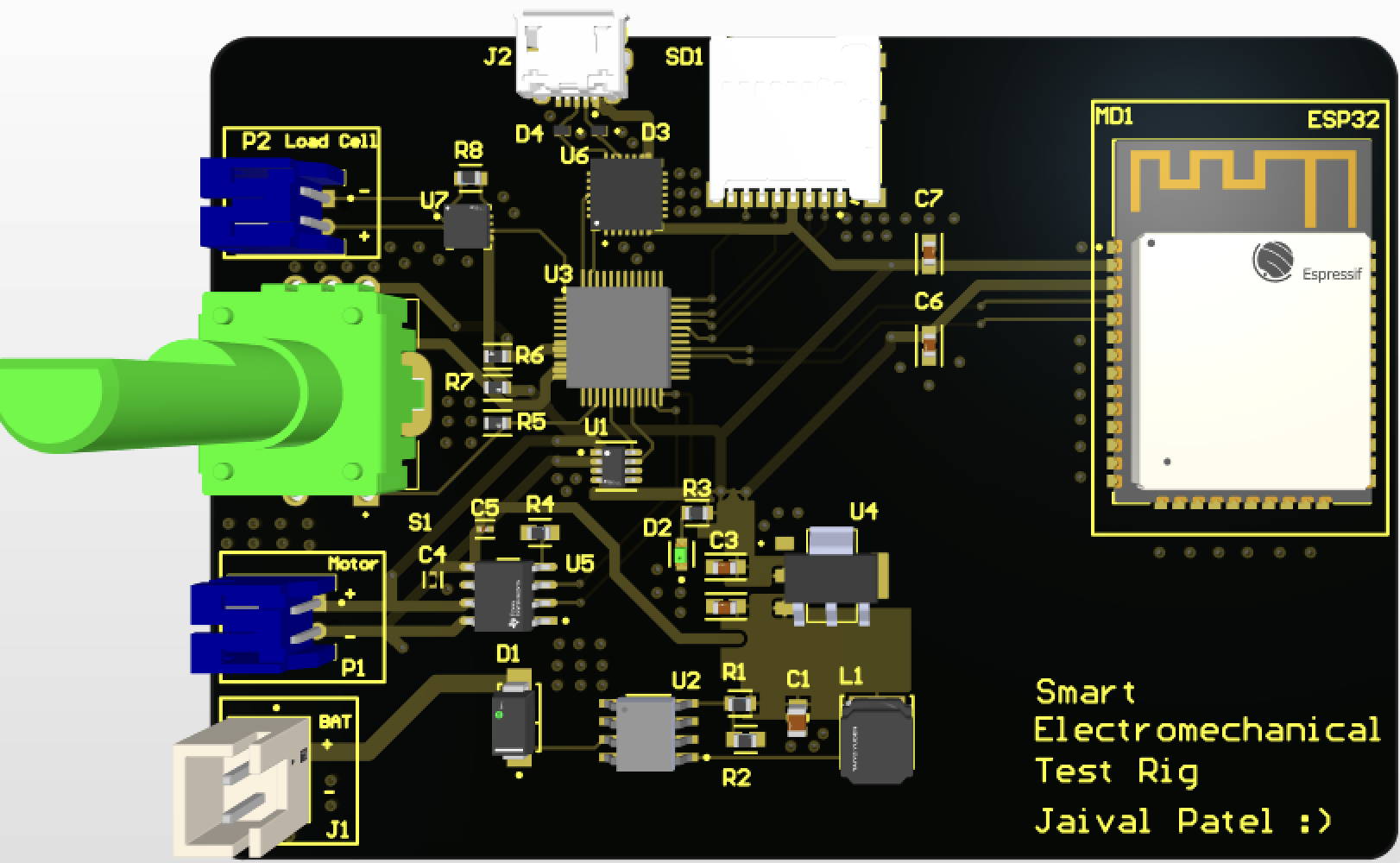
ESP32-WROOM-32E
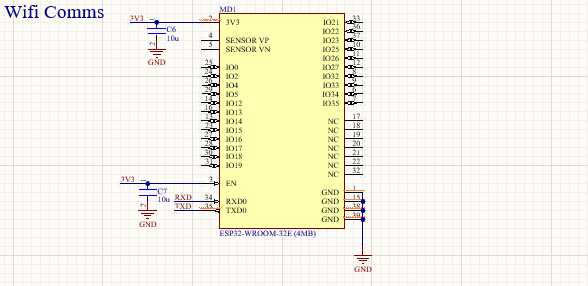
The ESP32 was chosen as the central MCU due to its dual-core performance, integrated Wi-Fi + BLE support, and rich peripheral set including I2C, SPI, UART, ADC, and SD/MMC interfaces. The WROOM-32E variant provides RF shielding, integrated flash, and stable operating temperature range for lab-to-field transition. Compared to STM32 or nRF52 families, ESP32 offered better support for real-time BLE and Wi-Fi mesh frameworks while maintaining deep sleep current under 10μA.
The ESP-IDF ecosystem allows fine-grained control over power domains and memory mapping. In this rig, one core handles sensor acquisition and SPI communication, while the other handles BLE streaming or SD logging.
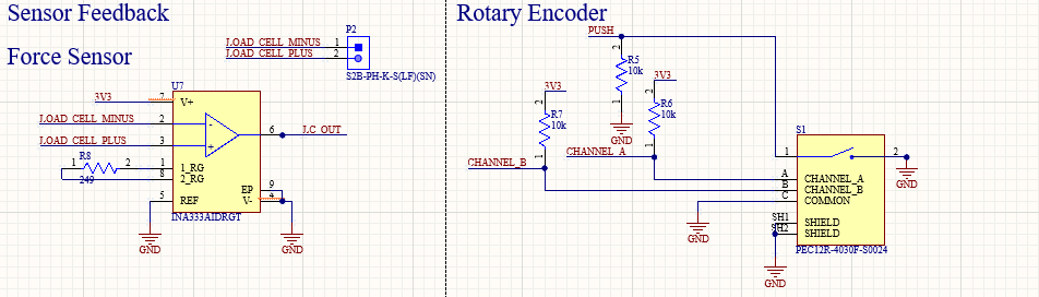
NA219 Current Sensor
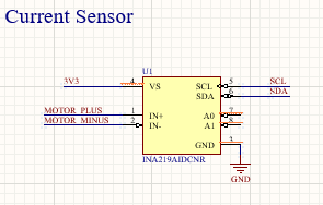
For current sensing, we selected the INA219 due to its I2C interface, integrated 12-bit ADC, and programmable gain amplifier. Unlike analog Hall-effect sensors, INA219 provides true differential sensing with millivolt accuracy. It also measures both voltage and current, allowing real-time power consumption profiling. The decision to use this over INA226 was based on board space and simplicity: the INA226, while more accurate, required additional filtering and SPI bus integration.
To improve sensing fidelity, Kelvin routing was used with matched trace lengths from the shunt resistor. All sense lines were shielded by ground pours and separated from the switching regulator path.
microSD Data Logging
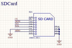
A key design feature was onboard data logging via SPI-connected microSD. We opted for SPI mode instead of SDIO due to easier firmware support and pin compatibility with ESP32 development boards. The microSD connector includes built-in card detection, ESD clamping, and reverse-insert protection.
To ensure reliable write performance, a decoupling capacitor bank (10uF + 0.1uF) was placed near the VCC pin. Data is buffered in RAM and flushed periodically to reduce wear and voltage ripple during long logging sessions.
LED Status Array
The board includes a 4-LED RGB indicator array tied to dedicated GPIOs. Each LED represents one of: power status, recording state, error/fault, and BLE connectivity. We avoided PWM flicker issues by driving them via open-drain outputs and using small resistors with controlled gate switching slopes.
Battery Voltage Monitoring
The battery voltage is divided via precision resistors and fed into an ADC input pin of the ESP32. A series diode and RC filter smooth out transient spikes and prevent ADC latch-up from reverse polarity events. This voltage is then used to report low battery conditions and initiate automatic sleep.
Bluetooth Streaming
BLE GATT profile was implemented to send sensor values, timestamps, and SD logging status to a paired smartphone or dashboard. We used the ESP-IDF NimBLE stack for its low memory footprint and reliable event queue management. The BLE profile is auto-initialized after system boot and deactivates during SD flush events to save power and avoid SPI contention.
PCB Layout Strategy
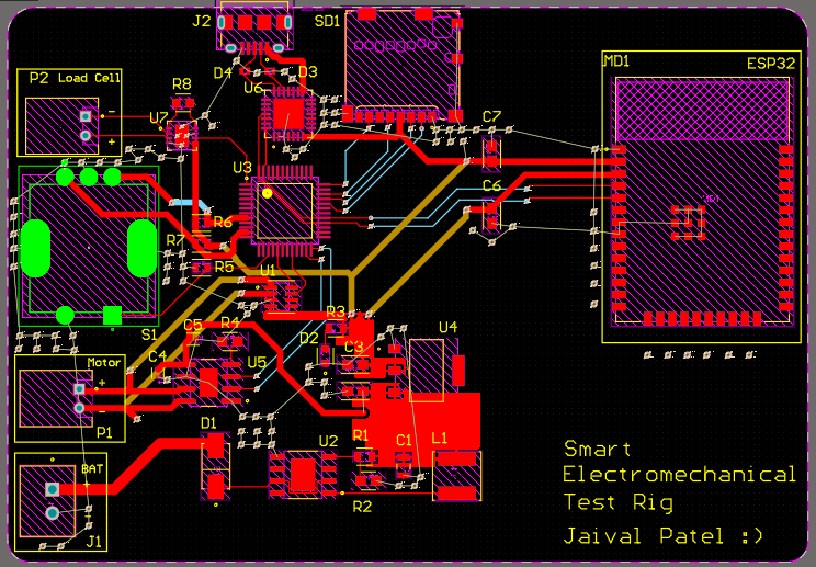
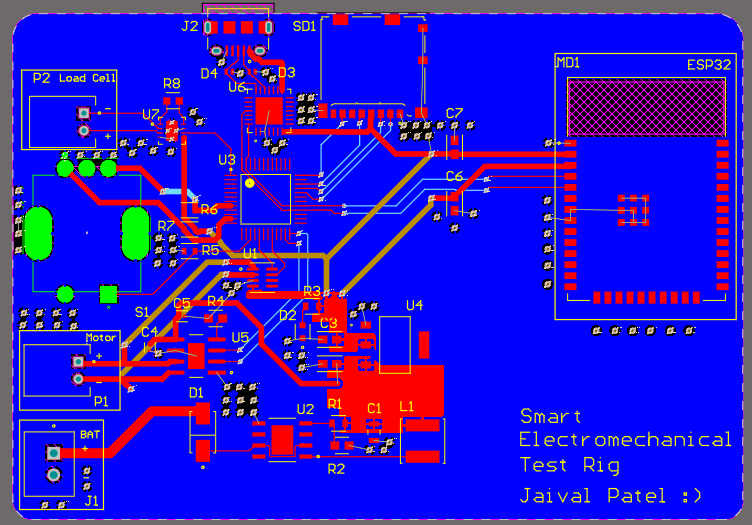
Layout for the Testing Rig was performed using KiCad 7 on a 2-layer FR-4 board with dimensions 70mm x 45mm. The layout reflects key principles of signal integrity, low-noise analog design, RF shielding, and mechanical serviceability.
Functional Zoning
The board is divided into four zones: power regulation, sensing and ADCs, microcontroller + logic, and I/O headers. This allowed simpler validation, easier debugging, and better analog/digital isolation.
Grounding & Pours
A full GND pour was implemented on bottom layer, stitched with 0.8mm vias near decoupling caps and component VSS pins. Ground planes were sectioned: analog GND under INA219 and ADC inputs, digital GND under ESP32 and SPI lines. This minimized return current overlap and ensured clean analog baselines.
Sensor Routing Strategy
All INA219 shunt traces were routed as short differential pairs with spacing ≤ 10 mil. Trace resistance was matched, and copper width was adjusted to keep temperature rise below 5°C under max expected current. SPI traces to SD were routed with 45° bends and length-matched to within 0.5mm to preserve clock edge stability.
Test Points and Debug Pads
A 6-pin UART header and 3 test points (3.3V, GND, VBat) were exposed on the board edge for oscilloscope probing. Boot and reset lines from the ESP32 were routed to pushbutton footprints with optional pull-up jumpers. I2C debugging could be done via test pad breakouts near the header area.
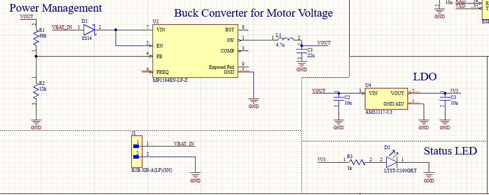
Power Management & Routing
The main power input was routed through a reverse-polarity diode and into a buck converter IC (MP2315). Output ripple was minimized with parallel MLCCs and a ground-return stitched directly under the inductor. All high-current traces were at least 60 mils wide and mirrored across layers using pour-connected vias.
LED and Visual Feedback Zone
LEDs were placed in the upper-left region with clear silkscreen symbols. Resistors were kept close to MCU GPIOs and grounded via individual vias to prevent shared return noise. This ensures accurate logic state feedback even during switching events.
Challenges & Debugging
1. SD Card Boot Timing
One of the earliest challenges was ensuring the ESP32 correctly initialized the SPI bus and mounted the SD card on boot. In early prototypes, the card would occasionally fail to initialize due to improper pull-up resistors and RC filtering on the CS and CLK lines. The SD card required 10k pull-ups on the MISO line and a 100nF capacitor on VCC to suppress inrush current from rail bounce at startup. In later revisions, SPI CS was routed to a GPIO with strong internal pull-up and manually reset before FS mount.
2. Power Ripple and Sensor Drift
When the board began SD write cycles, the INA219 reported sudden dips or spikes in current values. This was traced to ripple on the shared 3.3V rail during card I/O transactions. We fixed this by adding a dedicated LDO for the INA219 power supply, decoupling the sensor from high-frequency digital load switching. Additional 10uF MLCCs at the INA219 and SD slot helped stabilize the rails.
3. LED Logic Flicker
The status LED array initially flickered under simultaneous BLE and SPI operations. GPIOs shared timers, and switching between PWM and digital writes led to brief misfires. The fix was to assign fixed hardware PWM channels and buffer transitions via a queue-based state manager in firmware. A mild low-pass RC filter was also added to the common cathode rail.
4. BLE Transmission Conflicts
BLE packets were dropped during high-frequency logging, especially when SD transactions overlapped with BLE stack intervals. We restructured the firmware to schedule BLE updates only between SD transactions, and prioritized tasks using FreeRTOS event flags. Asynchronous ring buffers ensured no packet loss during SPI contention.
5. Physical Layout Constraints
The rig was dimensionally constrained to fit inside an existing enclosure. Early iterations suffered from connector crowding and GPIO overlaps. A rotation of the ESP32 footprint and mirrored header rows reduced cable crossovers and allowed more compact wire routing.
Tools & Skills Used
- Altium– Schematic & layout
- ESP-IDF – Real-time data capture, SPI + I2C drivers, BLE stack
- Logic analyzer – SPI validation & current sense calibration
Future Work
- IMU Integration: Add a 9-axis IMU (e.g. MPU9250) with interrupt-driven motion detection for mechanical stress mapping and resonance tracking.
- Touchscreen UI: Integrate a small SPI display + capacitive touchscreen to allow standalone configuration of test protocols, logging frequency, and thresholds.
- Battery Curve Estimation: Use INA219 data to log discharge profiles over time and fit predictive models of battery health (Coulomb counting, Peukert curve fitting).
- Isolation Amplifiers: Add isolation amplifiers on input lines for industrial-grade signal protection, enabling safe probing of high-voltage actuators or motors.
- Open-Sourced Dashboard: Build a React or Qt dashboard that can ingest BLE packets and visualize real-time plots, device health, and data exports.