EEG Neural Wearable
Overview
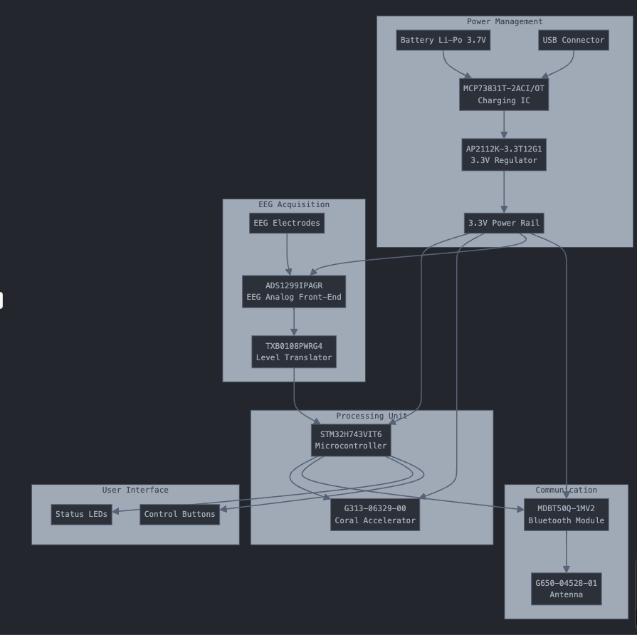
The EEG Neural Wearable is a compact, multilayer embedded system designed to classify human hand movements based on EEG brain signals. The project fuses low-noise analog signal acquisition, microcontroller-based processing, Bluetooth communication, and embedded machine learning into a single wearable platform. My goal was to explore how embedded systems can support real-time brain-computer interface (BCI) applications in a form factor small enough to be worn during typical daily activity.
PCB Design
EEG Acquisition – ADS1299IPAGR
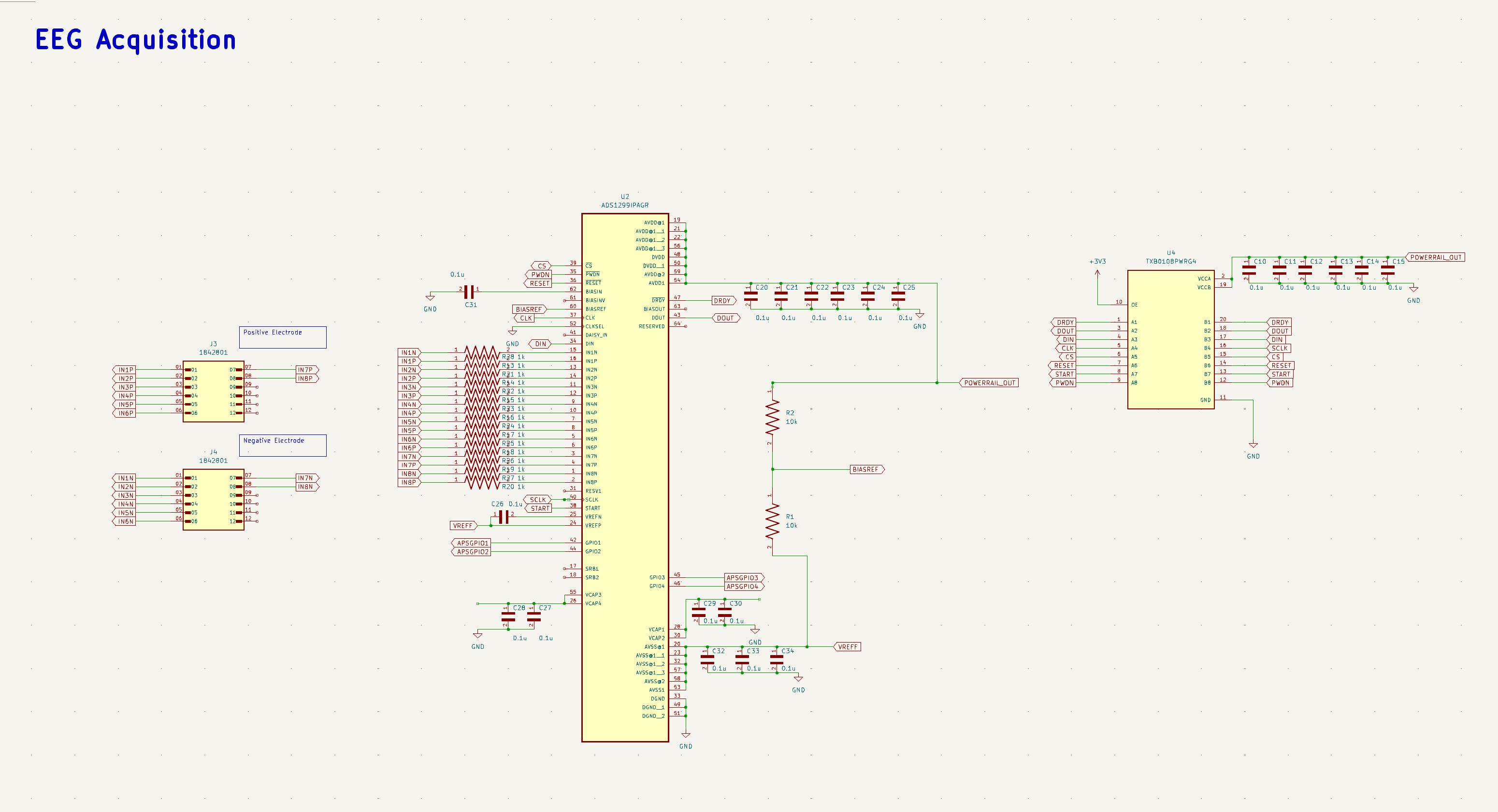
The Texas Instruments ADS1299 was selected as the core front-end because it is specifically designed for low-noise biopotential measurements (e.g., EEG, EMG, ECG). Its 24-bit resolution and integrated PGA make it suitable for detecting microvolt-level variations, and the SPI interface ensures simple communication with most microcontrollers. I chose the IPAGR package variant to minimize board footprint while allowing up to 8 input channels.
I considered the ADS1298 and the INA333-based discrete amplification, but ultimately favored the ADS1299 due to its compact integration, known use in open-source EEG systems (e.g., OpenBCI), and reduced component count for low-noise analog routing.
Processing Unit – STM32H743VIT6
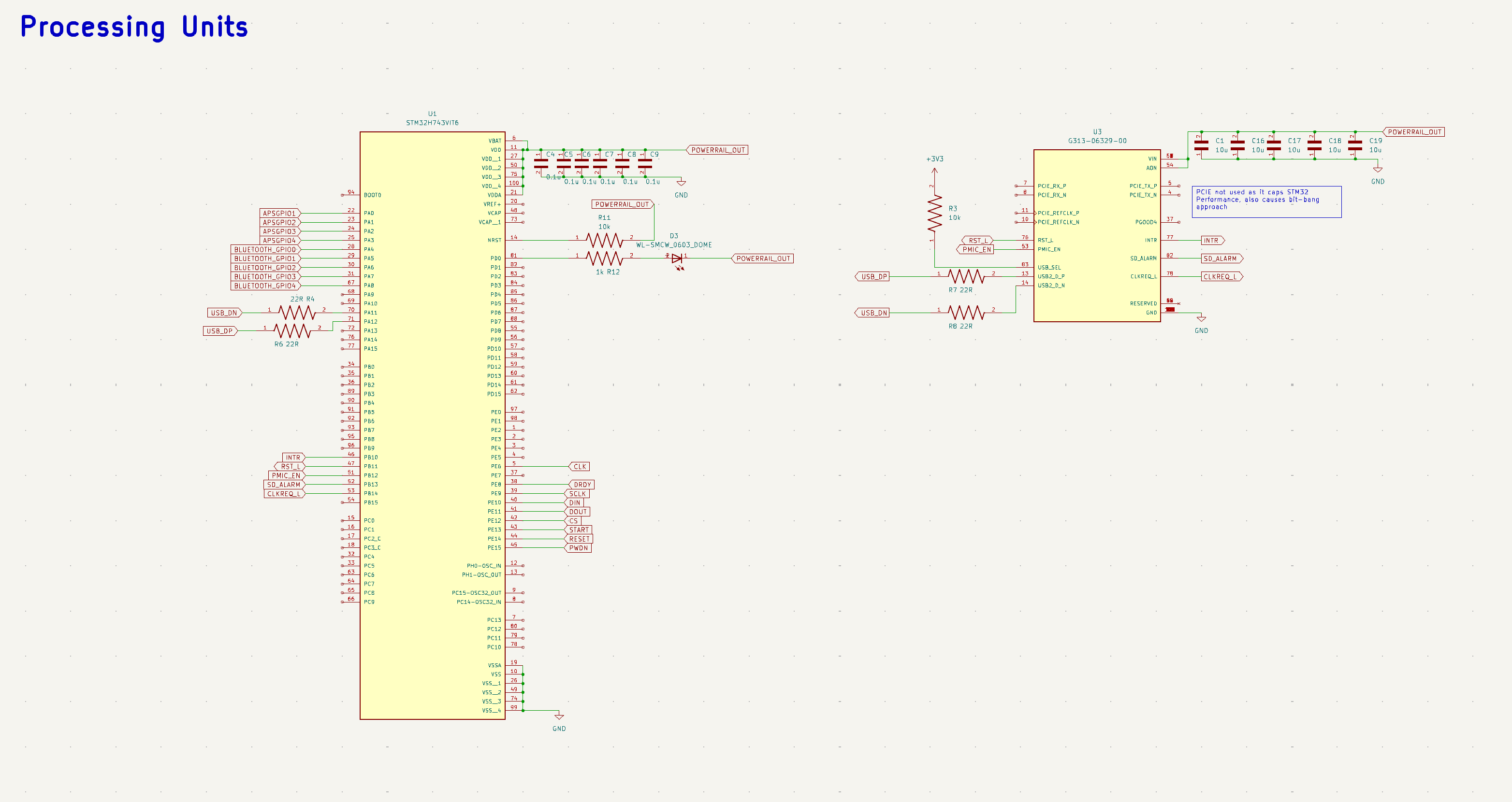
I chose the STM32H7 line for its balance of performance and integration. With a 400 MHz Cortex-M7 core, it provides ample headroom for FFT-based signal processing and real-time inference using a lightweight CNN model. It supports SDIO, USB, and external flash while maintaining low idle power.
The STM32F4 and ESP32-S3 were considered but lacked the needed RAM and true floating-point performance. The H7’s extensive peripheral availability also made it ideal for integrating SPI (to ADS1299), UART (for debug), SD card (for data logging), and USB.
Wireless Comms – MDBT50Q-1MV2 (nRF52840)
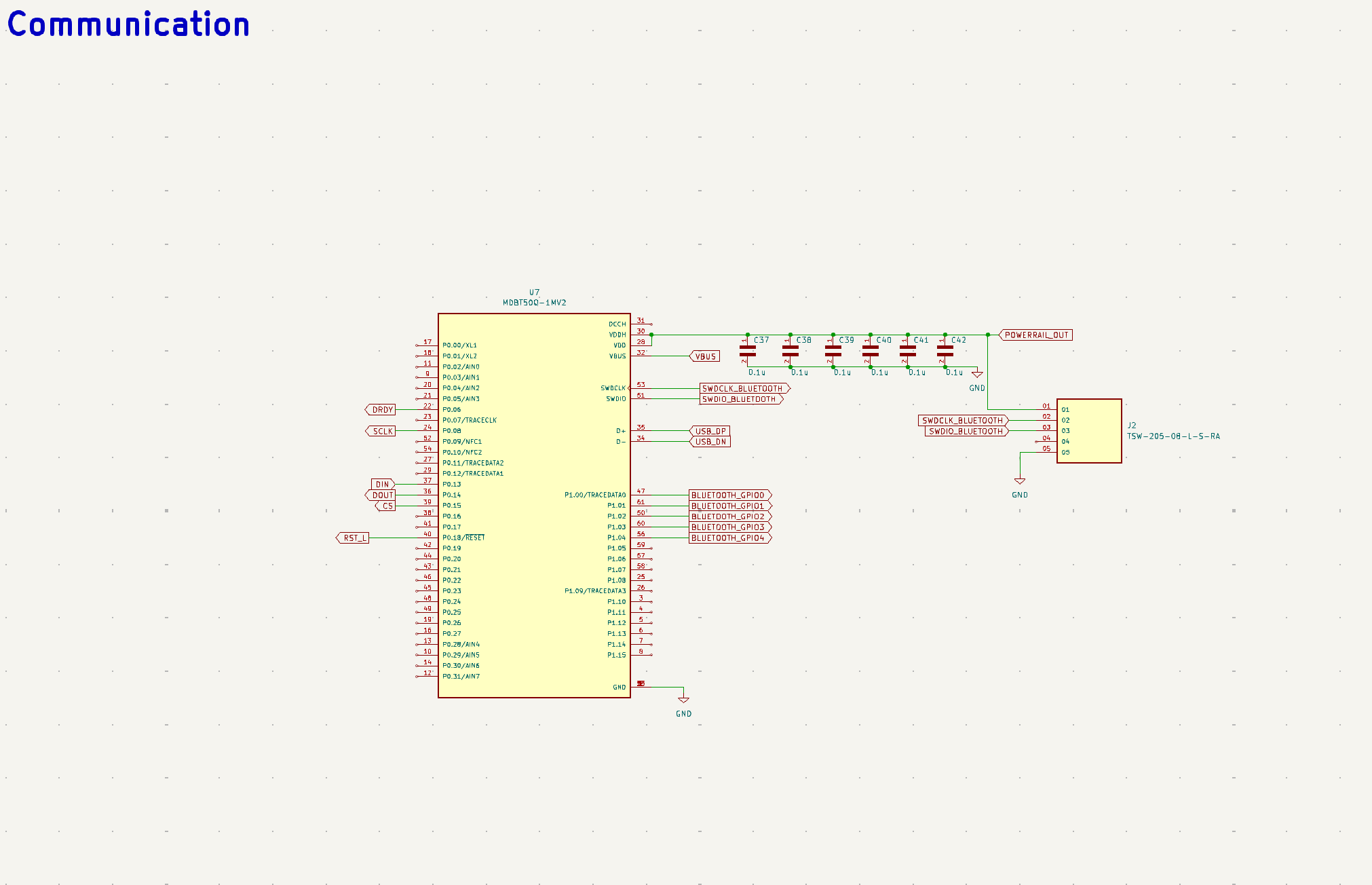
For BLE transmission, the MDBT50Q was selected as it offers a certified nRF52840 module with internal crystal and antenna. This drastically simplified RF design and bypassed the need for impedance matching. The module supports BLE 5.0 and offers more GPIOs than typical low-cost BLE SoCs.
An alternate design using the HM-10 BLE module was discarded due to its limited configurability and incompatibility with simultaneous SPI/UART comms.
Power Management
The power stage consists of:
- MCP73831 for Li-ion charging
- AP2112K-3.3V for low-dropout regulation
- Dual-source selection between USB and battery
The AP2112K was chosen for its low quiescent current and ease of sourcing. It ensures a clean 3.3V rail across the digital and analog domains. To avoid noise from buck converters, linear regulation was preferred despite efficiency tradeoffs.
I ensured analog and digital grounds were split and carefully stitched near the power entry point. All power traces were widened and kept short for voltage stability.
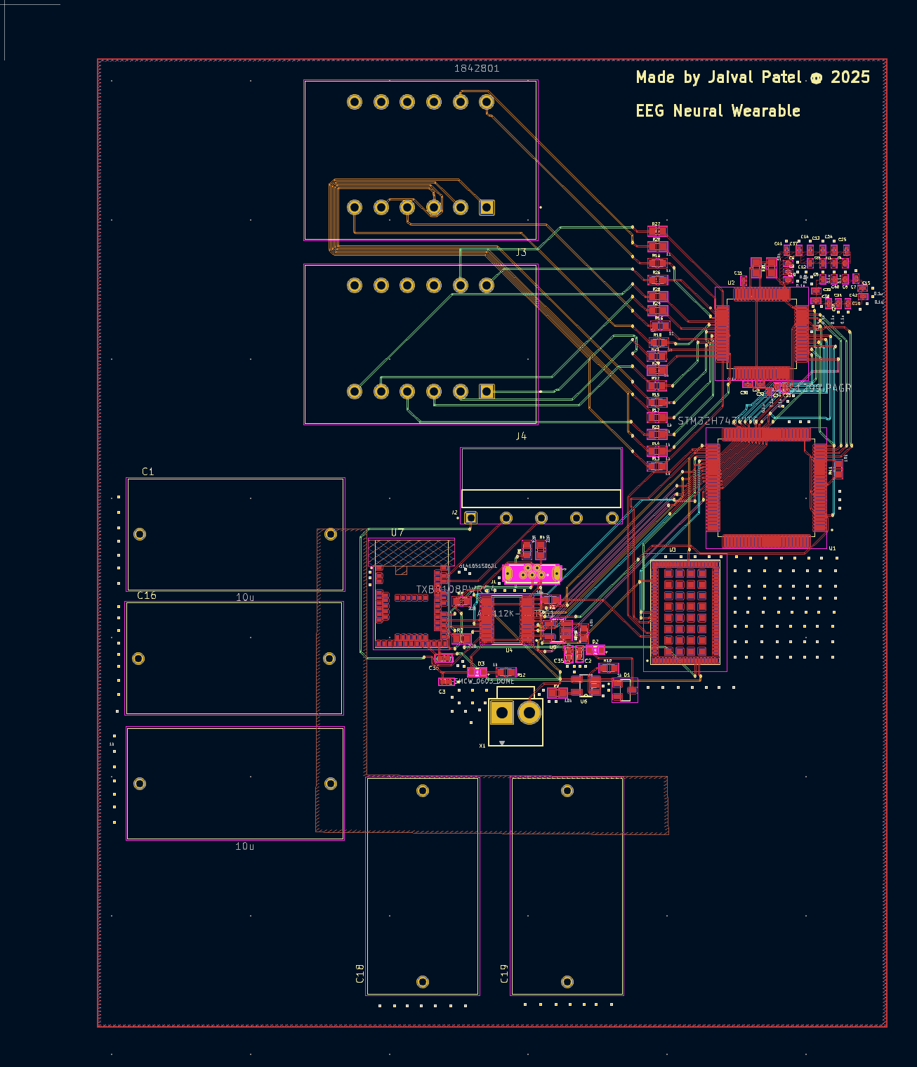
PCB Layout Strategy
The PCB was laid out using KiCad and features:
- 2-layer board for simplicity and cost
- Modular blocks for EEG, power, comms, and MCU
- Separated analog/digital ground planes
- Decoupling capacitors placed as close as possible to IC supply pins
- Test points for critical debug signals (e.g., SPI lines, RESET, DRDY)
ML Pipeline
ML Repo.To classify hand movements (left, right, circular), I used real EEG data from 3 users. Each signal was 14 channels sampled at 128 Hz. The key steps were:
- FFT (0–30Hz): Extract frequency domain features
- Waveband Aggregation: Average power in delta, theta, alpha, and beta bands
- Feature Structuring: 14 (channels) × 4 (bands) × 2 (mean types) = 112 features
This compact 112-length vector served as input to a CNN with:
- 3 convolutional layers
- Dropout = 0.3
- Categorical crossentropy loss
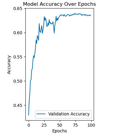
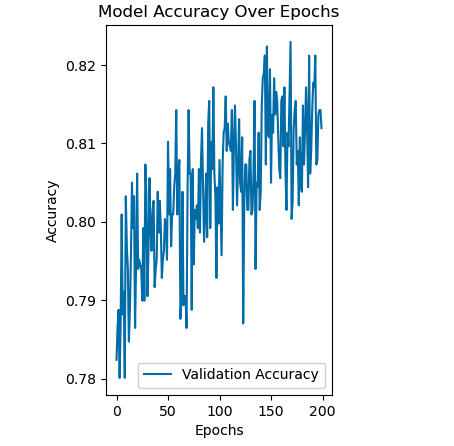
- Trained over 50 epochs, batch size = 32
CNN achieved 81.2% accuracy, while XGBoost slightly outperformed at 83%. Future models could include recurrent components or SVM baselines for better temporal resolution.
Challenges & Limitations
- Board Noise Management: Despite analog/digital separation, the 2-layer board is inherently noisier than a 4-layer solution. Power ripple and shared planes limited signal clarity during high-speed SPI bursts. Future revisions could include a solid GND plane and separate 3.3VA/3.3VD regulators.
- BLE Bandwidth: The BLE module occasionally bottlenecked high-throughput streaming. Workarounds included reducing transmission frequency and compressing payloads, but in a real application, UART-over-BLE or Nordic SDK optimization would be necessary.
- Board Size: Though wearable, the board could be made smaller with a 4-layer design and more compact components (e.g., switching from QFP to BGA packages, replacing JST headers with board-edge contacts).
- Model Generalization: EEG signals vary per user. The model, while effective for three test subjects, may need continual retraining or calibration. Future work could explore adaptive learning, model pruning, or federated learning pipelines.
Future Work
- Porting model to CMSIS-NN for real-time embedded inference
- Developing a mobile dashboard for data visualization
- Adding onboard flash for signal buffering
- Refining analog routing for higher CMRR and lower ripple