RF Signal Conditioning & Communication Board
Overview
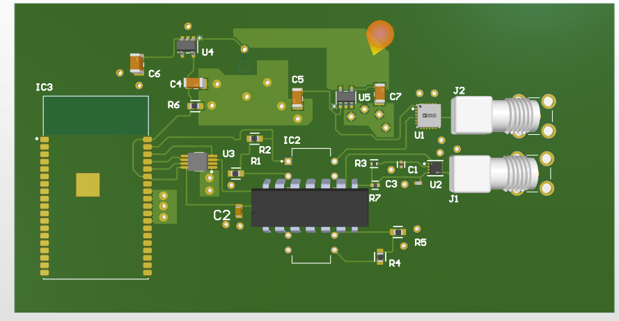
This project involved the development of a communication and RF signal conditioning board intended for wireless monitoring of coated microwave sensors. The board was designed to acquire RF signal strength from a custom microwave sensor, amplify and condition it using programmable analog circuitry, and transmit signal metrics wirelessly to a mobile application via Bluetooth. It integrates multiple functional subsystems including power management, digital potentiometer-based tunable gain stages, an RF power detector (LTC5597), and BLE communication using the ESP32-WROVER module.
Monitoring RF-based chemical sensors requires compact, tunable readout systems that can adapt to varying environmental conditions while remaining low power and wirelessly accessible. Most RF sensor setups are constrained to benchtop test equipment or lack embedded integration.
Our goal was to:
- Build an embedded system that amplifies and digitizes RF power output from a microwave sensor
- Allow gain tuning through software (digital potentiometer)
- Enable wireless communication with a mobile dashboard
- Operate on battery power and fit into a palm-sized form factor
Role
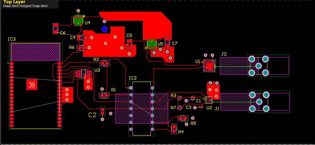
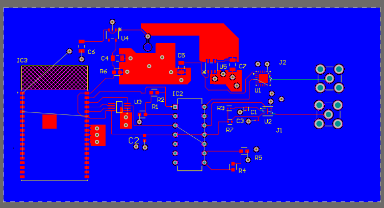
- Led schematic and PCB layout development in Altium
- Selected and integrated key analog components (MCP4141, LM324, LTC5597)
- Interfaced the ESP32-WROVER module with amplifier outputs and BLE services
- Iterated on layout changes based on faculty review comments
- Created and revised block diagrams and architectural flow
Key Features & Design Decisions
ESP32-WROVER-I – Wireless Communication
I chose the ESP32-WROVER-I for its robust BLE 5.0 support, integrated antenna, and dual-core processing capabilities. Compared to modules like the HC-05 or HM-10, the ESP32 provides significantly more flexibility, including OTA updates, Wi-Fi fallback, and low-power modes. Its SPI bus was essential for driving the MCP4141 digital potentiometer. Additionally, it allowed seamless integration with a mobile app dashboard under development.
Why not ESP8266? Lacked BLE and sufficient GPIOs.
Why not external BLE SoC? Increased complexity and required inter-IC protocol development.
MCP4141 Digital Potentiometer
This chip gave us software-controlled analog tuning, allowing real-time gain adjustment without physical intervention. It supported SPI control with 256-step resolution and operated comfortably at 3.3V, compatible with the ESP32.
Placed close to amplifier output and VCO input for tight gain loop.
SPI routing was kept short and isolated from analog signal paths to prevent switching noise injection.
LM324 Quad Op-Amp
The LM324 was chosen for its availability, single-rail operation, and stable bandwidth for low-frequency analog buffering. While not ideal for high-speed RF work, it was used to buffer control voltages, create gain stages for DC signals, and drive the VCO input.
Used in non-inverting amplifier and voltage follower configurations.
Carefully decoupled and placed away from high-frequency digital lines.
LTC5597 Power Detector
Selected due to its broadband RF input range (up to 40GHz) and ease of conversion to DC output. This part was critical for measuring the RF strength from the sensor. Its layout followed Analog Devices’ guidance: short RF traces, a clean analog ground plane, and precise decoupling.
Positioned close to SMA input to minimize loss
Output filtered and buffered before feeding into the ESP32's ADC
Power Regulation
Used linear regulators to avoid switching noise. Provided isolated 3.3V and 5V domains for clean digital and analog supply. Routed with wide copper traces.
Why discrete regulators?
- Provided better thermal separation
- Allowed independent rail filtering
- Gave the option to isolate analog/digital domains in future iterations
PCB Layout Strategy
- RF trace minimization: High-frequency traces between the SMA connector and LTC5597 were kept short and as straight as possible. Ground pours were placed around these lines for shielding.
- SPI bus isolation: The digital potentiometer's SPI traces were shielded with guard ground traces to prevent digital crosstalk from affecting the analog frontend.
- Power plane separation: Analog and digital grounds were split and stitched at a single point. This was especially important to keep ESP32 switching currents out of the sensitive RF measurement loop.
- Thermal dissipation: Copper pours were extended beneath regulators to provide passive heat sinking. Vias were added to move heat to the opposite layer.
- Connector orientation: All external ports (SMA, power input, debug headers) were placed on the board edge and aligned to simplify enclosure mounting and signal probing.
Note the second iteration also introduced a frame-based layout structure to ease PCB manufacturing and panelization with fiducial markers, text clearance zones, and consistent mounting hole spacing.
Challenges & Constraints
- Mixed-Signal Noise Management
- The ESP32 introduced high-frequency noise into the system. Despite careful grounding, there were moments of voltage ripple affecting analog readings.
- Solution: added bulk and ceramic capacitors near sensitive analog blocks, and extended analog trace spacing from switching regulators.
- VCO Interfacing Complexity
- Tuning a VCO via a potentiometer chain required buffering stages, but the impedance mismatch caused erratic behavior in early tests.
- Later stages incorporated voltage followers and damping resistors.
- No access to shielded lab for RF testing during prototyping
- Late-stage BOM and layout changes added routing pressure
Future Work & Improvements
- EMI Shielding: Add grounded copper enclosures over the LTC5597 and potentiometer chain to reduce ambient RF interference.
- Auto-Gain Control Loop: Use ADC feedback to adjust the MCP4141 resistance based on signal strength, stabilizing readings during environmental drift.
- Switching Regulator Redesign: ncorporate buck converters with well-filtered outputs to improve battery efficiency while maintaining analog cleanliness.
- OTA + Flash Logging: Add SPI Flash and integrate full over-the-air firmware updates with data buffering and fault-tolerant log recovery.
- Differential Signal Conditioning: Replace LM324 with a proper instrumentation amplifier front-end with higher CMRR for future analog sensor input options.
- Layout Modularity: Separate analog subsystem onto its own daughter board with edge connectors to allow RF experimentation without affecting digital logic.
- Design and deploy a Flutter-based mobile dashboard for remote tuning