CDAQ-EEG
Overview
This project involved developing a compact, multilayer embedded system for real-time neural data acquisition and edge processing. The design focused on acquiring EEG signals with high fidelity, preprocessing onboard with an STM32 microcontroller, and wirelessly transmitting sensor outputs over BLE for real-time interfacing. Though the machine learning model is a planned next step, this project lays the full hardware and systems groundwork for embedded BCI use cases.
Traditional neural recording systems are often tethered to benchtop setups or suffer from poor wireless fidelity and power efficiency. To move toward next-generation BCI architectures, there's a clear need for miniaturized, low-noise, battery-powered systems capable of real-time sensing and computation. This project targets that gap, providing a reconfigurable node architecture capable of supporting edge neural classification in future iterations.
Key Features
The CDAQ-EEG board was engineered as a modular, real-time biosignal acquisition platform for embedded neural processing. Every design decision was informed by noise reduction, system-level modularity, power efficiency, and wireless fidelity for brain-computer interface (BCI) applications. Though this version does not yet run an onboard classifier, all hardware and signal paths were optimized to support eventual edge machine learning on the STM32 microcontroller.
ADS1299 – Analog Front-End for EEG
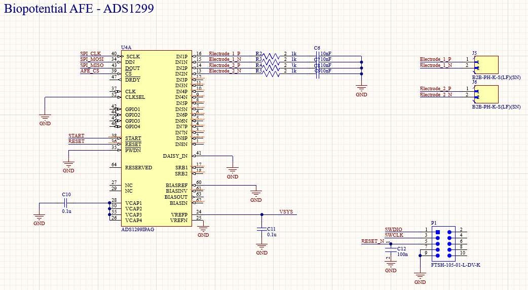
The ADS1299 from Texas Instruments was selected as the EEG acquisition IC due to its 24-bit resolution, differential input configuration, and integrated programmable gain amplifier. Compared to discrete op-amp stages or lower-resolution ADCs, the ADS1299 dramatically simplifies EEG front-end design by providing fully-integrated bias generation, electrode impedance measurement, and internal reference voltage.
The IPAGR package was chosen for its reduced footprint and ease of soldering on a 4-layer board. This choice enabled compact routing while preserving signal integrity with short, symmetric trace lengths between the electrodes and the AFE input pins.
I avoided using alternate front-ends like the OpenBCI-compatible ADS1298 or INA333 cascaded systems due to poorer integration, lower channel count, and more complex calibration requirements.
STM32H743VIT6
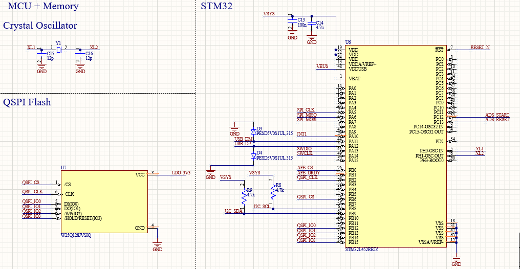
The STM32H7 series was selected for its 400 MHz Cortex-M7 core, integrated FPU, and ample RAM (1 MB SRAM) — essential for buffering multichannel biosignals and supporting real-time FFT or filtering. Its high-speed SPI peripheral allows full-bandwidth data capture from the ADS1299 (up to 32 kHz across 8 channels), while DMA and RTOS support allow parallel logging and BLE streaming.
The decision to use this device over an STM32F4 or ESP32 was driven by its better floating-point performance and direct support for CMSIS-NN if a future CNN is deployed. The QFP package was also easier to assemble and debug than BGA-based STM32H7s while offering breakout of all peripherals.
MDBT50Q-1MV2 – BLE Module (nRF52840)
For wireless streaming, the MDBT50Q was selected due to its onboard antenna, RF shielding, and certification compliance. Built around the Nordic nRF52840 SoC, it provides BLE 5.0 support and additional GPIOs for optional control logic. The integrated antenna eliminates the need for matching network tuning and saves routing complexity for 2.4 GHz paths.
The module connects to the STM32 via UART for BLE telemetry and configuration commands. The decoupled architecture allows independent firmware stacks for neural data acquisition and wireless communication.
Power Management
The power subsystem includes:
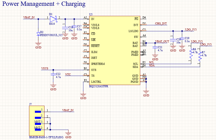
- MCP73831 for Li-ion battery charging
- AP2112K LDO for clean 3.3V regulation
- Schottky diode isolation between USB and battery rails
Linear regulation was selected over buck converters to eliminate switching ripple near the EEG front-end. Although less efficient, this decision significantly reduced baseline noise observed on the ADS1299. Ground planes were separated and stitched near the power input connector, with analog and digital domains isolated during layout.
USB-C Interface
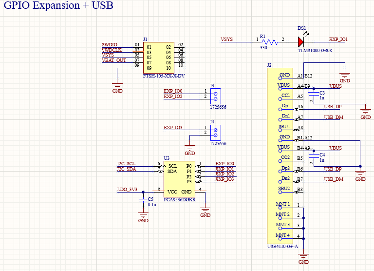
The board includes a USB-C interface using the Amphenol USB4110-GF-A connector, which supports both power delivery and full-speed data communication. This connector was chosen for its rugged through-hole mounting, compliance with USB 2.0 standards, and ability to handle mechanical strain in wearable or field setups.
The USB-C interface serves as both a firmware flashing/debug port (via STM32's USB FS peripheral) and a high-throughput data output channel when BLE bandwidth is insufficient. CC pull-down resistors (5.1kΩ) ensure correct role detection, and ESD protection was added to safeguard the D+/D− lines during hot-plug and transport.
This interface significantly improves developer workflow by enabling direct serial access and bulk data retrieval from the STM32 over USB, acting as a fallback or complement to wireless streaming.
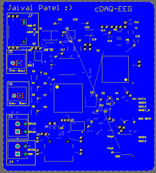
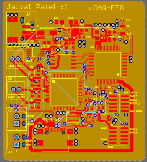
PCB Layout Strategy
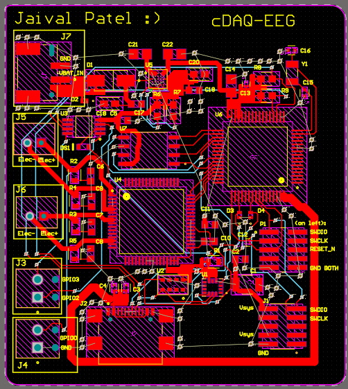
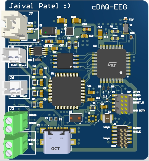
The CDAQ-EEG board was laid out as a 4-layer PCB to accommodate high-density analog routing, noise separation, and a reliable ground return network. Layers were assigned as: Top – Signal, L2 – GND, L3 – 3.3V Power Plane, Bottom – Signal. This stackup allowed minimal return path impedance, reduced EMI, and maintained trace width control for critical signals.
Analog Front-End Routing
The ADS1299 analog input traces were kept as short, symmetrical differential pairs from the EEG header to the IC input pins. High-impedance traces were routed away from any digital lines and surrounded by ground pours for shielding. RC low-pass filters (10k + 100pF) were placed within 2mm of each input pin to reduce aliasing and protect against ESD.
Power and Ground Strategy
The ground layer (Layer 2) was uninterrupted and used as the reference plane for all signal returns. Analog and digital domains were separated with their own pours and stitched near the power entry point via a star ground configuration. This prevented high-frequency digital switching currents from interfering with the analog measurement loop.
The power plane (Layer 3) was dedicated to 3.3V distribution with branch segmentation to ADS1299, STM32, BLE, and USBC domains. Decoupling caps were placed <1mm from each IC’s VDD pin and tied to the internal power plane via short vias.
BLE Antenna Clearance
The MDBT50Q was placed along the board’s edge with no copper under its antenna footprint on any layer. A 6mm clearance zone was enforced around the antenna area and marked in mechanical layer. No signal traces were routed near the antenna zone, and the nearest stitching via was >4mm away to prevent detuning.
SPI Routing
The SPI bus from STM32 was routed on the bottom layer with short stubs, matched-length traces, and ground shielding. Clock and data lines were grouped and routed as tightly coupled pairs to minimize EMI. Decoupling and series termination resistors were tuned via scope measurements to avoid overshoot during long bursts.
High-Speed Signal Isolation
STM32-H7’s SPI and UART lines were routed as controlled impedance lines over the GND plane to maintain edge quality. Data and clock lines were separated from ADC analog traces by at least 5mm, with layer transitions only made when necessary via blind vias.
Mechanical Considerations
The board outline (60x50mm) was selected to fit within a wearable sleeve enclosure. All connectors and status LEDs were placed along the periphery for accessibility. Screw terminal pads were added for electrode headers with adequate silkscreen spacing for manual connection in a lab environment.
Challenges & Debugging
SPI Bus Instability
During initial bring-up of the ADS1299, the SPI MISO line returned inconsistent data under load. Analysis via logic analyzer showed irregular SCLK-to-MISO timing. This was traced to simultaneous contention on SPI CS lines and ground bounce due to shared digital return path. A dedicated analog ground plane with star-stitching to digital ground resolved timing jitter. Additionally, I added a 47Ω series resistor to the SCLK and MISO lines to minimize ringing and improve signal integrity.
BLE and STM32 Boot Conflict
The MDBT50Q BLE module attempted UART communication during STM32 startup, which caused unexpected behavior due to shared reset vector bootstrapping. I added a GPIO-based startup delay mechanism where the BLE module holds off until STM32 asserts a ready signal. This ensured sequential boot and preserved the UART bus for dedicated logging and streaming.
Thermal Hotspots Around Regulators
The initial use of a switching regulator created audible coil whine and heat rise near the analog input section. Ripple measured on VDD exceeded 30mVpp during SD writes, which degraded the noise floor of EEG signals. Swapping to an LDO-based regulation path (AP2112K) and increasing copper pour area improved thermal dissipation and reduced switching artifacts.
Antenna Detuning from Pour Intrusion
Early revisions mistakenly allowed copper under the BLE antenna on inner power layers. This caused reflection, packet loss, and significantly reduced range. The fix involved enforcing keep-out zones across all four layers using mechanical drawings, and validating antenna performance using an RF sniffer.
Tools & Skills Used
- Altium – Full schematic + multilayer layout
- LTspice – Simulation of EEG input and front-end transient behavior
- STM32CubeIDE – Firmware scaffolding for acquisition, logging, BLE sync
- BLE sniffer, logic analyzer – Debug and protocol validation
Future Work
- Deploy CNN-based classifier using CMSIS-NN on STM32
- Add onboard flash ring buffer for long-term telemetry
- Miniaturize board for wearable/implant-scale applications
- Develop mobile app to pair with BLE stream and visualize EEG traces