CAN Node Emulator
Overview
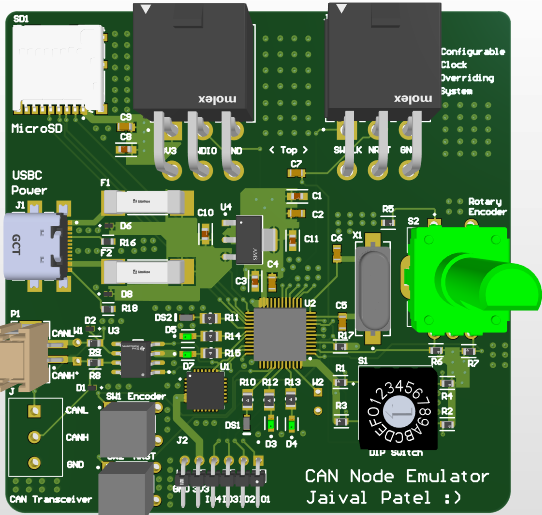
The CAN Node Emulator is a multilayer STM32-based hardware platform that emulates multiple Electronic Control Units (ECUs) over a shared CAN bus. This custom board was built to serve as a diagnostic, prototyping, and fault injection tool for automotive systems testing. Designed to support real-time message scheduling, arbitration, and subsystem emulation, it plays a critical role in test automation and validation pipelines for modern electric vehicles and distributed embedded networks.
Traditional ECU test benches rely on expensive modular simulators or manually-configured hardware that lacks flexibility. This project was driven by the need to build a portable, reconfigurable, and open CAN node emulator that can support the development and testing of in-vehicle networking systems such as powertrain controllers, BMS units, and drive-by-wire subsystems.
Key Features
The CAN Node Emulator was built as a reconfigurable platform to simulate the behavior of ECUs on a shared CAN bus. Every component was selected to support accurate message generation, precise timing, low-level fault emulation, and robust physical communication. This section outlines the rationale behind selecting each major hardware feature.
STM32F103C8T6 Microcontroller
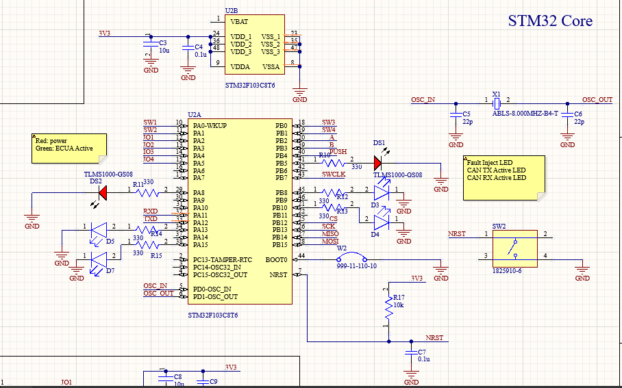
The STM32F103C8T6 was selected as the main controller due to its native support for CAN 2.0B through the bxCAN peripheral. It operates at 72 MHz with enough SRAM and flash to buffer message queues, emulate multiple node states, and support real-time I/O toggling. The microcontroller also includes built-in USB FS functionality for DFU flashing or CDC communication.
Compared to alternatives like ATmega328P or ESP32, the STM32 offers hardware message filtering, interrupt-driven CAN handling, and better compatibility with the ISO 11898 physical layer. The availability of ST’s open-source CubeMX tools and debugger support further facilitated development.
SN65HVD230 CAN Transceiver
The SN65HVD230 from Texas Instruments was chosen for its automotive-grade reliability, integrated TXD dominant state timeout, and ability to operate in high-speed (1 Mbps) or silent mode. It meets ISO 11898 standards, offers ±12kV ESD protection, and has superior common-mode noise tolerance compared to MCP2551 or other legacy transceivers.
Placing the transceiver near the edge-mounted screw terminal minimized stub length and maximized bus signal integrity. A second footprint was added to optionally test simultaneous multi-node arbitration using firmware-toggled transceiver enable logic.
ECU Message Scheduling and Simulation
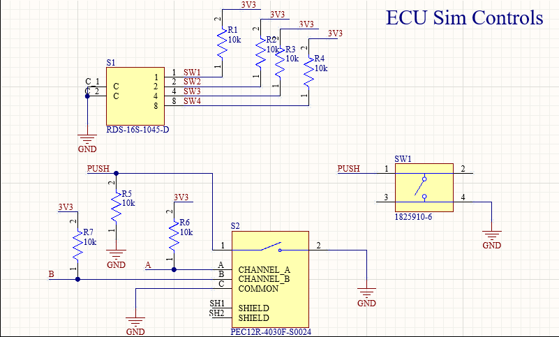
The firmware on the STM32 is designed to support replayable or time-triggered message frames, enabling it to simulate periodic messages from ECUs such as BMS nodes, torque controllers, or infotainment systems. Messages can be loaded from DIP switch profiles or streamed over USB. Timing is synchronized via a hardware timer and CAN interrupt flags.
The emulator can enter silent mode to passively observe bus traffic or inject error frames to simulate bad checksum or bus-off states. This behavior is crucial for testing node recovery and safety fallback in larger vehicle subsystems.
Power Regulation Subsystem
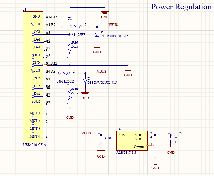
The 5V power input from the USB-C connector or external header is stepped down using an AMS1117-3.3 LDO. The regulator was selected for its simplicity and robust thermal behavior in lab conditions. Though less efficient than buck regulators, the linear topology provided low ripple during logic operation and reduced EMI during oscilloscope testing.
All decoupling capacitors were placed <2mm from VCC pins of key devices, and a copper pour was included around the regulator with thermal vias for proper heat dissipation. A reverse protection diode and polyfuse on the 5V rail prevented overcurrent damage during hot-plug events.
PCB Layout Strategy
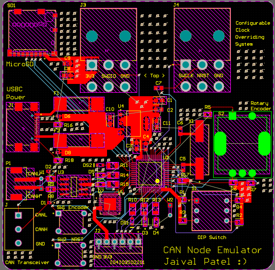
The CAN Node Emulator uses a 5-layer stackup tailored for robust signal integrity and power domain separation, reflecting best practices drawn from high-reliability automotive designs. Layout decisions emphasized trace isolation, bus compliance, manufacturability, and debug access—factors essential when targeting test systems that mimic real-world subsystems found in vehicles developed by Tesla and similar firms.
Board Dimensions and Mounting
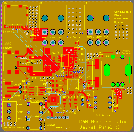
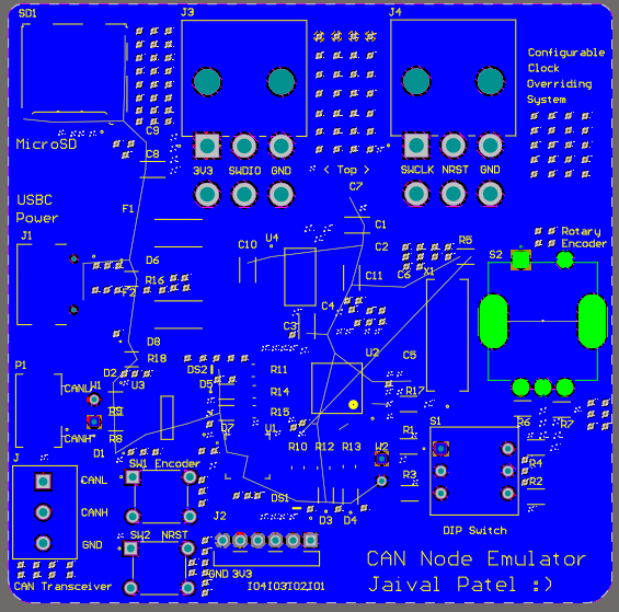
The board measures 70mm × 50mm and includes four M2 plated mounting holes. These were added not only for mechanical securing but also to interface directly with aluminum-backed enclosures or shielding compartments. The mechanical holes are connected to the ground plane to allow potential chassis grounding and EMI suppression via metal standoffs.
Layer Stackup
The layer arrangement is as follows:
- Top Layer: Component placement and critical routing (CAN signals, reset logic, debug)
- Layer 2: Split power planes (5V entry and 3.3V local rails)
- Layer 3: Continuous GND plane for signal return integrity
- Layer 4: Secondary signal routing (UART, USB, config logic)
- Bottom Layer: Headers, optional SD interface, and D+/D− USB routing
CAN Bus Routing
CAN_H and CAN_L were routed as tightly coupled differential pairs with 120Ω termination near the edge-mounted screw terminal. Traces were matched to within 0.15mm and kept free from stubs. Transceiver outputs were routed directly to the terminal with only one via transition and zero layer crossings. Adjacent digital logic traces were kept at least 6mm away to avoid differential impedance degradation.
USB-C and High-Speed Signal Placement
USB-C D+/D− traces are routed as a matched pair using microstrip geometry over the GND plane. A clearance zone of 4mm surrounds these lines on L1 and L4, and the connector’s shield tabs are connected to GND using via stitching to suppress radiated noise. Signal entry is filtered via ESD protection (PESD3V3L1BA) located <5mm from the connector pads to meet USB 2.0 transient response targets.
Power and Thermal Strategy
The linear regulator (AMS1117-3.3) has its output plane mirrored on both L2 and L4, with thermal vias connecting its pad to an internal copper island. Power filtering uses 10uF ceramic caps near all decoupling points and ferrite beads to reduce ground bounce across subsystems. A wide trace fanout distributes power to transceiver, DIP switches, and logic IO while maintaining <10mV ripple under 300mA peak load.
DIP Switch and Configuration Routing
The DIP switch array is placed along the top edge and connected via 10k pull-ups to 3.3V. Each switch pin passes through a low-pass RC filter before reaching the STM32 GPIO. Traces are kept under 30mm in length, free from adjacent toggling signal paths, and labeled with silkscreen references for intuitive test scripting.
Component Placement and Clearances
The STM32 is centered to minimize trace lengths to USB, CAN, and boot configuration pins. The transceiver is placed within 10mm of the CAN terminal block to reduce loop area. Status LEDs are aligned on the lower edge for external viewing through an enclosure cutout, while debug headers are aligned for right-angle cable insertion during test fixture use.
Challenges & Debugging
1. CAN Bus Contention and Arbitration Testing
One of the most complex challenges in this project was emulating multiple ECUs on a shared CAN bus without causing contention or bus errors. When two transceivers were simultaneously active with dominant arbitration frames, collision windows would occur that exceeded the acceptable arbitration delay margins. This was addressed by configuring the STM32 firmware to selectively activate one transceiver at a time and by enabling silent monitoring mode on passive transceivers to reduce active drivers. Proper bus termination with a 120Ω resistor network at the terminal block helped further stabilize arbitration.
2. ESD and Hot-Plug Transients
In field test simulations, hot-plugging CAN cables induced noise bursts that corrupted logic states or brownout-reset the MCU. We introduced clamping protection on CAN_H and CAN_L using PESD3V3TVS diodes and added a common-mode choke at the bus entry point to suppress differential transients. This configuration, used in many OEM ECU designs, ensured bus stability under dynamic cable insertion.
3. USB-C and Flashing Consistency
The USB-C interface uses the same electrical structure as other portfolio boards — based on the USB4110-GF-A connector, with ESD protection and a 5.1kΩ CC resistor for device role negotiation. However, we encountered enumeration issues on some hosts due to insufficient pull-down impedance. A 1MΩ discharge path from CC to GND was added and capacitor decoupling near D+/D− was tuned to meet full-speed USB eye-diagram margins.
4. microSD Compatibility
Although this project uses the same microSD hardware setup as previous boards (SPI mode, card detect line, and filtered VDD), we encountered compatibility issues with newer high-speed cards. This was resolved by slowing the SPI clock during initialization and increasing the CS-to-data setup delay. A 10uF + 0.1uF cap pair on the VCC line, along with series resistors on SCK and MOSI, helped stabilize signal edges and reduce CRC mismatch errors.
5. DIP Switch Debounce and Configuration Latency
The mechanical DIP switch array introduced bounce-induced misreads during configuration load. Adding an RC low-pass filter (10k + 1nF) per input line, along with software debouncing (3 reads spaced at 5ms intervals), improved reliability. This ensured deterministic startup behavior, crucial for repeatable test scenarios.
6. Boot Pin Conflicts with USB and UART
Early testing revealed that the BOOT0 pin conflicted with USART1 TX logic during flashing mode. This was corrected by reassigning debug UART to USART2, isolating BOOT0 behind a jumper with pull-down logic. Now, firmware can be flashed reliably using either USB DFU or ST-Link without interfering with runtime serial output.
Tools & Skills Used
- Altium Designer – Schematic and 5-layer PCB layout
- STM32CubeMX + STM32CubeIDE – Peripheral configuration and firmware logic
- CANalyzer, Saleae Logic – Real-time CAN signal analysis and protocol validation
- Oscilloscope, function generator – Signal injection and transient characterization
Future Work
- Implement replay-based simulation with timestamped log playback
- Integrate ML model for anomaly detection and ECU behavior clustering
- Add USB-C CDC bridge for host-controlled injection over CAN
- Miniaturize layout for in-vehicle stealth deployment