Custom Battery Management System (BMS)
Overview
This custom Battery Management System (BMS) was designed to support embedded applications requiring secure, multi-rail power delivery, battery monitoring, and protection switching logic. The board integrates real-time telemetry, robust power integrity, and onboard diagnostics for use in hardware test environments, robotics, or wearable electronics.
Off-the-shelf BMS modules rarely offer the degree of customizability needed for R&D hardware setups. I aimed to build a tailored BMS that:
- Provides 3.3V and 5V regulated rails from a single-cell Li-Ion source
- Monitors voltage, current, and thermal faults at runtime
- Enables safe switching between USB and battery input
- Isolates analog and digital grounds to minimize noise
PCB Design
Power Regulation
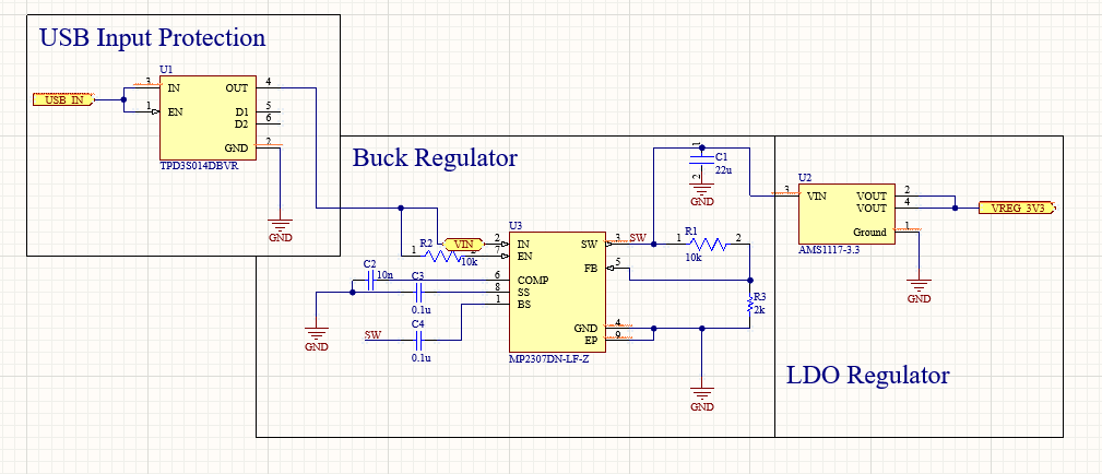
Chosen for its 95% efficiency, low quiescent current, and high switching frequency, reducing inductor/cap size.
Additionally, the AMS1117-3.3 linear regulator was selected for its simplicity, low dropout (1.1V max), and widespread availability. It powers the MCU and low-voltage analog circuitry. Decoupling capacitors (10uF tantalum and 0.1uF ceramic) were placed at the output pin to suppress high-frequency noise.
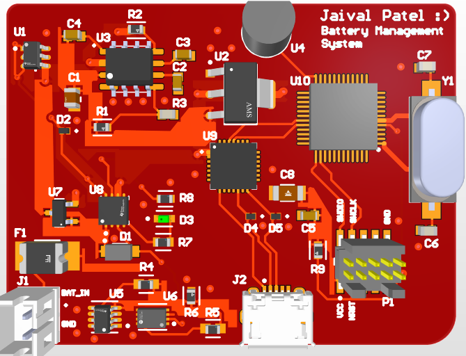
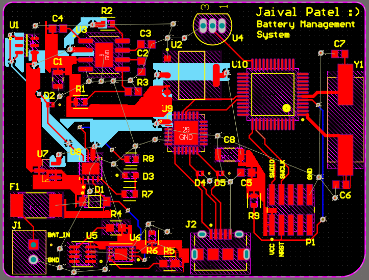
Board Placement: Situated near the STM32 microcontroller, with minimal trace length to VDD pins. Grounded copper pour beneath improved thermal dissipation.
Power Path Switching
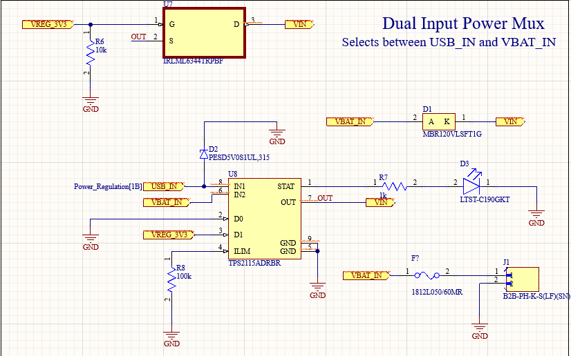
A dual-MOSFET plus ideal diode arrangement ensures seamless transition between USB and battery without brownout. Gate drive logic is derived from voltage sense rails.
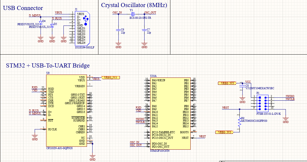
I selected the IRF7406 N-channel MOSFET due to its low RDS(on) and robust SO-8 package. It supports drain-source voltages up to 30V and continuous drain currents over 5A, which suited our battery's 2S configuration. The gate was driven by a discrete gate driver circuit to ensure fast turn-on/off transitions, reducing switching losses.
Board Placement: Positioned close to the battery input to minimize trace inductance. A TVS diode was placed at the drain to suppress inrush current spikes and connector transients.
Battery Monitoring
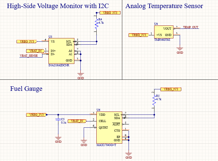
Precision resistive dividers with op-amp buffering were used to feed battery voltage into an MCU ADC. A current sense resistor and INA219 allow for runtime energy tracking.
The INA219 was chosen as the current and voltage monitoring IC due to its I²C interface and ability to sense currents via a low-side shunt resistor. Its internal 12-bit ADC enabled accurate readings without needing an external ADC on the MCU.
Located directly adjacent to the shunt resistor and load path to avoid trace resistance errors. The SDA/SCL lines were routed with controlled impedance and series resistors to mitigate ringing.
Regulation Strategy
Used buck regulation for 3.3V and LDO for analog sections to ensure high PSRR and low ripple near sensor interfaces. Inductor placement was isolated from analog sections to reduce EMI coupling.
Standard 5-pin SWD (Serial Wire Debug) interface for STM32 MCU debugging was used. A 100nF capacitor was placed on the reset line to prevent brownout issues during power transients.
Board Placement: Accessible near board edge with through-hole header to simplify in-field flashing and debug access.
PCB Layout Strategy
The PCB layout for this custom Battery Management System (BMS) was designed with an emphasis on minimizing ground noise, optimizing heat dissipation, and maintaining clear separation between high-voltage switching paths and low-noise analog sections.
Board Partitioning
The board was laid out with modular zoning to isolate high-frequency switching sections from low-noise analog domains. I used a pseudo-star ground topology and routed the analog ground back through a high-impedance path to the shared GND stitching point. This ensured differential voltage stability across sensor circuits.
Power Trace Widths
I followed IPC-2221A guidelines to determine trace widths. For example, the 12V input path was routed with 60 mil traces (2 oz copper) to safely carry up to 2A. Each high-current net was mirrored with a solid ground return directly below, enhancing current loop compactness and reducing EMI.
Thermal Management
All power ICs were paired with thermal vias below their thermal pads, connecting to large copper pours on both sides. I also used exposed copper under the TPS5430 for passive heatsinking. These pours doubled as local ground planes to spread heat and decouple switching noise.
Routing Decisions
Differential pairs (I2C, UART) were tightly coupled and length-matched to reduce timing skew. Long analog traces were shielded using ground tracks on both sides, with no layer transitions to avoid discontinuities. Signal vias were kept away from return current paths to avoid crosstalk.
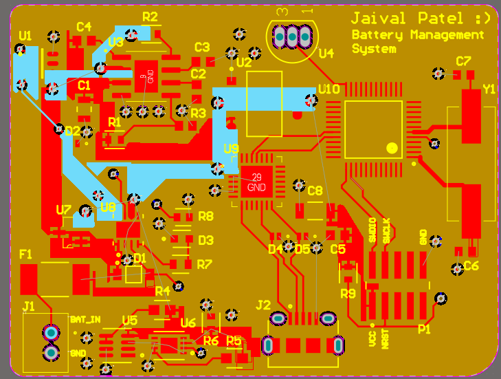
Signal traces were routed orthogonally across layers to minimize crosstalk. Analog and digital signals were kept on separate planes with grounded guard traces around ADC-sensitive lines. Differential traces (e.g., I2C) were impedance-controlled and matched in length within 5 mils to ensure synchronous communication under high load.
Extensive use of polygon pours connected to ground ensured low-impedance return paths and helped with EMI shielding. Decoupling capacitors were placed within 2mm of all IC supply pins and vias were stitched under ground planes to reduce parasitic inductance.
Challenges & Constraints
- Footprint Constraints: All components had to fit on a 2-layer board while maintaining isolation zones. Strategic via placement and staggered silkscreen was used to save space.
- Thermal Management: Passive cooling was prioritized; large ground pours and thermal vias were added beneath regulators.
- ADC Noise: Initial testing showed 15–20 mV ripple on analog ADC reads. This was mitigated by adding ferrite beads and increasing Cfilter values.
Future Work
- Add I2C EEPROM for fault log persistence
- Improve balancing circuit to support multi-cell Li-Ion configurations
- Expand telemetry protocol to UART/BLE