BLDC Motor Driver Board with FOC
Overview
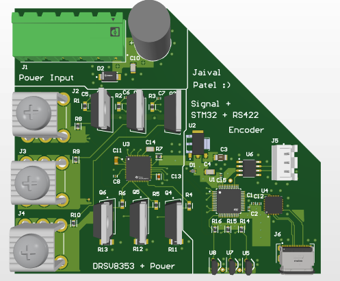
This project is a full-featured BLDC (Brushless DC) motor driver board designed around the Texas Instruments DRV8353RSRGZT smart gate driver. The system integrates all peripheral blocks needed for closed-loop motor control, including a UART debug interface, differential encoder inputs, Hall-effect position sensing, and a 3.3V regulation rail for logic. The project highlights my ability to design robust high-current switching hardware, manage system-level signal integrity, and integrate mixed-signal...
Objective
To develop a standalone motor driver PCB capable of handling three-phase commutation for BLDC motors up to 48V, while supporting external control via PWM/SPI and providing accurate feedback using Hall and encoder sensors. The system was optimized for modularity, noise resilience, and future expandability for use in robotics, mechatronics, and mobility systems.
Role
- Successfully controlled BLDC motor using STM32 PWM in 6xPWM mode
- UART output allowed real-time debug of DRV faults, phase voltages, and motor current
- Quadrature encoder A/B pulses decoded cleanly up to 50kHz
- System demonstrated in closed-loop velocity mode under load with minimal noise artifacts
Key Features
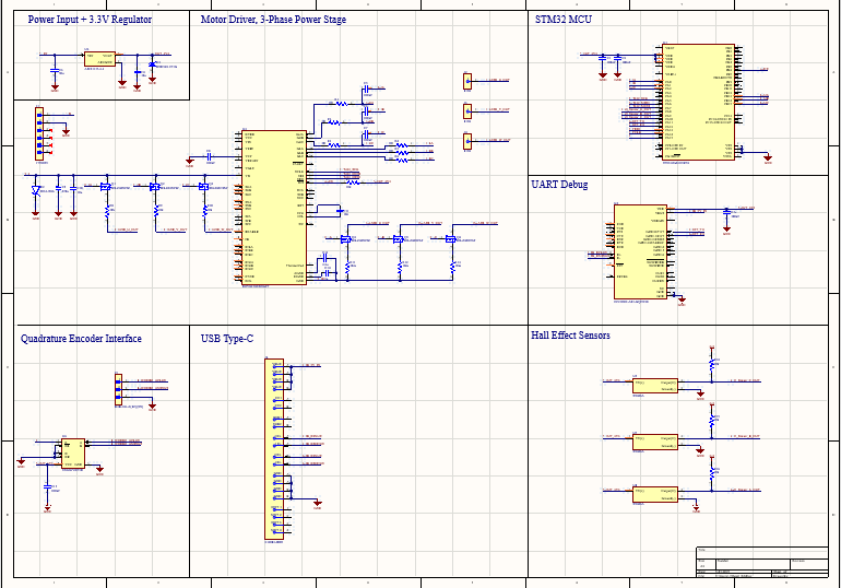
DRV8353RSRGZT Smart Gate Driver
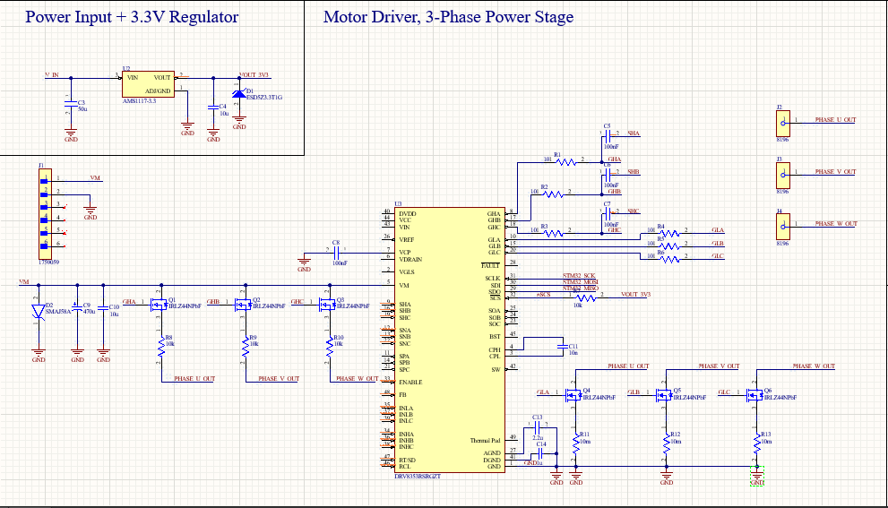
The DRV8353 was selected as the core of the gate drive subsystem after an extensive review of competing three-phase gate drivers from Infineon, STMicroelectronics, and Monolithic Power Systems (MPS). The key reasons for choosing this part were:
- Programmability via SPI: Compared to simpler DRV8305/8301 analog-driven variants, the DRV8353-RS offers SPI-based configurability. This was crucial for debugging, adaptive dead-time control, and fault response in development.
- Integrated Protection Features: It includes UVLO, OCP, SCP, and thermal shutdown, which significantly reduces external analog complexity.
- Flexible PWM Input Topology: The part supports 6x and 3x PWM mode selection, allowing the firmware to evolve from trapezoidal drive to FOC without hardware change.
- Low RDS(on) Bootstrap Configuration: The integrated bootstrap diodes reduce BOM size and simplify layout by removing discrete fast-recovery diodes.
Other options considered included:
- MP6536 (MPS): While highly integrated, it lacked SPI control and exposed fewer tuning parameters, making it less adaptable for advanced control modes.
- L6234 (ST): An older device requiring more external components and offering weaker thermal protection and current limit configurability.
- Discrete IR2110 Drivers: Rejected due to excessive complexity in protection and shoot-through timing implementation.
IRLZ44N N-Channel Power MOSFETs
The IRLZ44NPBF FETs were chosen for initial prototyping due to the following:
- Availability and Cost: Through-hole version readily available for hand-soldering and rework during test cycles.
- Logic-Level Gate Drive: Fully enhanced at 4.5V–5V, compatible with DRV8353’s gate driver outputs.
- High Pulse Current Rating: Capable of handling >30A pulsed currents, giving room for transient spikes during startup or commutation changes.
- Thermal Performance: D2PAK footprint provides low RθJA when heatsinked through copper pour and vias.
Alternatives explored included CSD18540Q5B and PSMN2R6-40YS, but these SMD FETs would have required reflow assembly and had longer lead times during supply chain constraints.
AMS1117-3.3 Linear Regulator
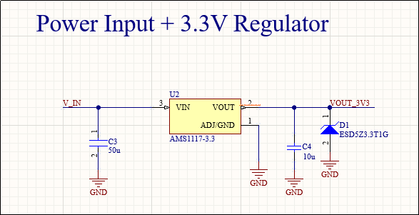
The AMS1117 was chosen over switch-mode regulators (like LM3671) for simplicity and EMI cleanliness. Key considerations:
- Low Component Count: Requires only two capacitors and handles up to 1A of load current—more than sufficient for the logic subsystem.
- Noise Isolation: No switching noise injected into sensitive analog signals or Hall effect decoders.
- Thermal Behavior: While inefficient at high ΔV, total dissipation was within limits (< 0.75W) under worst-case conditions with 9V–12V input.
CP2102N USB-UART Bridge
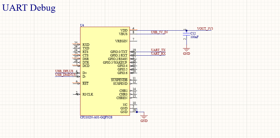
This chip enables host PC debug access without needing a separate USB debugger. Advantages included:
- Integrated Clock + EEPROM: No external crystal needed; device settings customizable via Silicon Labs software.
- Low Enumeration Time: Speeds up iteration cycles during firmware debugging.
- Proven Driver Support: Widely supported across OSes and dev boards.
SN65HVD75 RS-422 Receiver
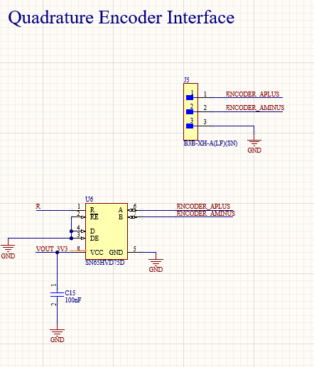
Encoder lines were routed differentially to maximize noise immunity. The SN65HVD75 supports:
- Up to 10 Mbps bandwidth, plenty for high-speed encoders
- Failsafe biasing on idle lines to prevent glitching
- Stable output swing over temperature
Chosen over basic line receivers like 74HC14 due to superior line termination and ESD protection.
Hall Sensor Input Block
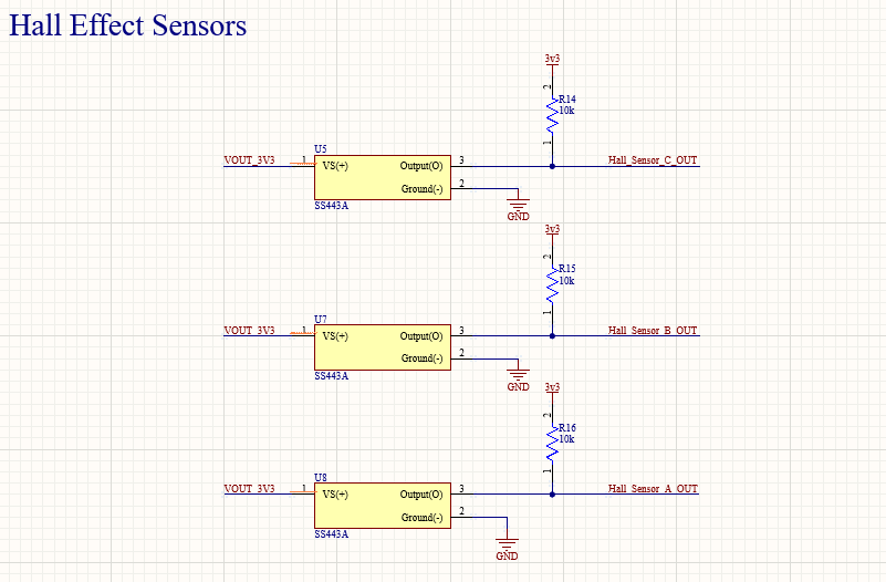
Passive RC filters and series diodes were used to protect against voltage overshoot from back-EMF coupling. Signal levels were tuned to STM32-compatible 3.3V logic, with fast edge rates preserved for accurate edge timing on digital inputs.
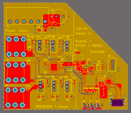
PCB Layout Strategy
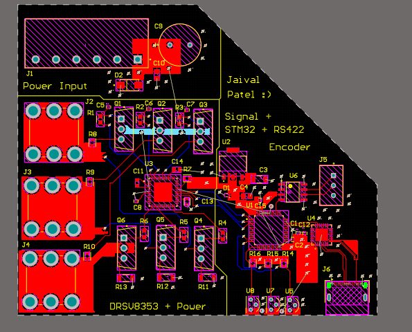
Placement Philosophy
- High-current switching nodes (phase outputs, FETs) placed closest to the gate driver
- Hall, encoder, and UART inputs grouped along a signal-side zone, routed orthogonally to prevent interference
- Power and logic domains physically separated with strategic polygon stitching
Power and Signal Domain Separation
The most fundamental layout decision was to physically and electrically separate the high-power switching stage (VM, phase outputs, FETs, DRV gate paths) from the sensitive low-voltage digital subsystem (UART, Hall, encoder, 3.3V logic). This reduced noise coupling between high di/dt transitions and slow digital edges, minimizing the potential for false triggering or EMI radiation.
Loop Area Minimization
Minimizing the loop area of high-current paths is essential for both electromagnetic compatibility and efficiency. The switching loop formed between high-side FET, phase node, low-side FET, and GND return was routed as compactly as possible by placing FETs close to the DRV IC and directly connecting them using wide polygon pours. The return path was mirrored on the second layer with extensive stitching vias to complete the loop and minimize inductance.
Polygon Pour Hierarchy
- GND Pour: Defined first, stitched across layers via grid of 0.8mm vias. Tied all low-side source pins, Hall/encoder shields, UART, and logic reference points.
- VOUT/PHASE Pours: Separated into distinct islands for each motor phase (U, V, W). Each routed from the midpoint of the FET pairs using wide traces and 2oz copper.
- VM Input Pour: Filtered input through TVS and MLCCs before polygon expansion. Care was taken to avoid placing noisy VM traces under analog or reference nets.
Placement by Functional Zone
- Top-left quadrant: UART + USB header + CP2102
- Top-right: 3.3V linear regulator and LDO filter network
- Center: DRV8353 + FET bank + bootstrap caps + gate resistors
- Bottom-left: Hall sensor connectors and input filters
- Bottom-right: Quadrature encoder A/B differential pair + SN65HVD75 + pull-up network
This separation facilitated focused routing, minimized net crossover, and ensured each subsystem had clean ground and power return paths.
Gate Trace Routing
Gate traces were kept as short as possible and directly routed from the DRV outputs to the MOSFET gates. Gate resistors were placed within 2mm of the gate pin to suppress ringing and overshoot. Layout included:
- Use of 45° turns to minimize impedance discontinuities
- No vias in gate traces to maintain signal edge integrity
- Local grounding of gate return pins to avoid shared inductive paths
SW Node Shielding
The SW node (phase switch point) is a major source of EMI. To prevent its radiation from coupling into feedback lines or MCU I/O, the SW node was:
- Kept compact using fat polygon-only fills
- Surrounded by guard traces and stitching to drain transient fields to GND
- Isolated on top layer with no digital routing allowed within a 5mm keep-out zone
Differential Pair Integrity (Encoder Lines)
The A/B encoder lines are routed as matched-impedance differential pairs from the SN65HVD75 input header to the MCU header. While this isn’t a true controlled-impedance board, traces were routed symmetrically, with equal lengths (within 20 mils), and referenced to continuous GND on the lower layer to suppress common-mode conversion.
Decoupling and Bypass Cap Layout
Every power input to the DRV8353, CP2102, AMS1117, and encoder receiver includes both bulk and high-frequency MLCCs. Decoupling caps were placed as close as possible to the power pins (within 1.5mm), and return directly to the nearest GND via. Bypass cap paths were verified for low ESL with direct routing to copper pours.
Silkscreen and DFM Considerations
Connectors are clearly labeled by function and polarity to assist integration. Designators do not overlap with via arrays or copper pour edges. Mechanical mounting holes were left with a soldermask ring and pullback clearance for potential standoff hardware.
PCB Stackup and Materials
2-layer FR-4 1.6mm board with ENIG finish. Copper thickness: 1oz by default, with selected regions (FET outputs, power plane) enlarged to 2oz via custom fab specification for higher current handling. Next version will move to 4-layer with internal GND and VM planes to further isolate return paths and boost thermal spread.
Challenges
Developing a high-performance motor driver board involves navigating a range of challenges — electrical, mechanical, layout, and systems integration. This section presents a deep analysis of the issues encountered throughout the design and build process and how they were methodically resolved or mitigated. The goal was not just to “get it working,” but to build a scalable, stable system grounded in sound engineering principles.
Switching Noise Coupling into Signal Traces
Problem: Initial tests revealed erratic behavior on Hall sensor outputs and encoder lines during high-speed PWM switching. The suspicion was cross-coupling from high dv/dt phase transitions into signal traces.
Root Cause: Poor spacing between high-side FET drain (SW nodes) and low-speed digital lines, along with a lack of shielding.
Solution:
- Moved all Hall and encoder signals to a tightly grouped “signal zone” on the opposite board edge
- Placed GND pours around and underneath all signal traces
- Added series RC filters on Hall inputs to suppress spikes without degrading edge detect accuracy
Ground Bounce and Shared Returns
Problem: Noise was seen on the 3.3V rail under load. The DRV’s gate current return was shared with the CP2102 UART ground plane, causing UART disconnections at startup.
Root Cause: Mixed analog and switching ground domains tied too closely without segmentation.
Solution:
- Isolated logic and power grounds using star topology, connected at a single plane near DRV GND pin
- Routed separate GND pour under UART/USB path
- Replaced GND trace links with full copper zones stitched via thermal vias
Power Dissipation in FETs During Stall
Problem: Under test stall conditions (low PWM frequency), MOSFET temperatures rose rapidly.
Root Cause: Gate drive strength was not optimized for switching speed, leading to increased overlap losses and conduction heating.
Solution:
- Used DRV8353’s SPI configurability to adjust gate drive current to high strength for rise/fall reduction
- Added copper planes under drain pads and tied them via thermal stitching to ground
- Reconfigured stall detection to cut PWM on extended zero-speed fault
Debug Interface Instability
Problem: UART messages were occasionally corrupted or dropped, especially during commutation events or rapid SPI updates.
Root Cause: CP2102 shares power rail with noisy DRV logic current and analog front end; voltage dips created brownouts.
Solution:
- Decoupled CP2102 power with low-ESR capacitor close to VDD pin
- Moved USB connector and CP2102 away from phase zone
- Implemented resend logic in debug terminal and MCU UART driver
DRV Fault Response Tuning
Problem: DRV8353 entered fault mode intermittently under load without clear diagnostic reason.
Root Cause: Overcurrent detection was set too aggressively and did not account for motor inrush at spin-up.
Solution:
- SPI register tuning based on expected Ipeak and inductive rise time
- DRV now logs fault codes over UART on trip and holds until host clears
- Documented current sense scale and trip margin based on layout parasitics and shunt tolerance
Silkscreen and Assembly Errors
Problem: During initial assembly, polarity errors were made due to ambiguous silkscreen on power and Hall sensor headers.
Solution:
- Revised silkscreen for all headers: added bold polarity marks and descriptive labels
- Added mechanical layer markers for standoff locations to aid in mechanical integration
Design Review and Iteration Strategy
Each board revision was reviewed against a checklist for thermal performance, functional isolation, testability, and integration. Key changes across versions:
- Version 1 → 2: Changed power plane routing and split logic GND from VM GND
- Version 2 → 3: Added encoder pull-up logic, thermal vias, silkscreen corrections, and UART RC filter
Tools
- PCB Design: Altium schematic/layout, polygon pours, DRC constraints
- System Integration: UART, SPI, PWM, analog sensing, ESD design
- Signal Integrity: Loop area management, impedance control, grounding
- Embedded Support: STM32 pinout planning, debug bus exposure
Future Work
- Add onboard STM32 microcontroller + buck converter for full system-on-board control
- Integrate INA240 or similar current sense amplifier to enable true torque loop control
- Design EMI filter on VM input to mitigate switching noise reflection
- Expand header compatibility for CAN, I2C, and other industrial interface standards
- Explore moving to 4-layer board to dedicate planes for power and signal return
PPO Deployment for BLDC Motor Driver
I have also deployed a Proximal Policy Optimization (PPO) policy onto a custom-designed high-voltage BLDC Motor Driver PCB. The system was built to enable real-time closed-loop motor control using reinforcement learning — with a focus on robotic applications such as humanoid locomotion, dynamic actuation, and torque adaptation.
Both the paper and the corresponding model repository can be found in the above links.
System Overview
- Microcontroller: STM32F103C8T6
- Inference Model: PPO-trained policy exported to TensorFlow Lite
- Inputs: Rotor position, velocity feedback, target trajectory angle
- Outputs: Motor PWM duty cycle commands for DRV8353 motor driver IC
Training Pipeline
The PPO agent was trained in simulation using Stable-Baselines3 in a custom MuJoCo environment that modeled BLDC motor dynamics and a reference trajectory task. The reward function penalized tracking error, overshoot, and power inefficiency — enabling robust adaptation to varied load conditions and dynamic setpoint changes.
Deployment
After policy convergence, the trained model was quantized and converted to .tflite format. It was deployed to the STM32 microcontroller running a custom embedded interpreter. The system executed inference in real time, taking sensor feedback as input and adjusting torque commands at millisecond intervals.
Key Results
- Latency: < 70 ms control loop including inference and actuation
- Model Size: ~38 KB post-quantization
- Tracking Error: < 2.5° average deviation from target trajectory
- System Power: Operates from 3.3V logic supply, ~55 mW at runtime
Significance
Deploying PPO directly to an embedded motor driver opens new possibilities for real-time learning-based control in robotics. Unlike traditional PID or FOC loops, the PPO policy adapts to disturbances, load shifts, and changing trajectories without re-tuning. This design enables