ASIC Fakeout Board
Overview
The ASIC Fakeout Board is a custom-designed emulation platform created to replicate the I/O behavior and power sequencing of an unreleased application-specific integrated circuit (ASIC). This board allows firmware developers and hardware engineers to begin system integration, test signal pathways, and validate voltage domains before the actual silicon is available. It ensures early-stage compatibility verification and accelerates product development cycles.
Key Features
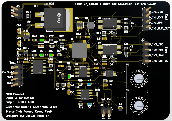
The ASIC Fakeout Board was developed to simulate and validate communication, isolation, and power conditions for a mock ASIC module during system-level bring-up and debugging. Each block was designed to mirror key ASIC interface behaviors using discrete components while providing safe test access, fault insertion capabilities, and flexible debugging pathways—critical for hardware-in-the-loop simulation pipelines in high-reliability systems.
CAN Telemetry Interface
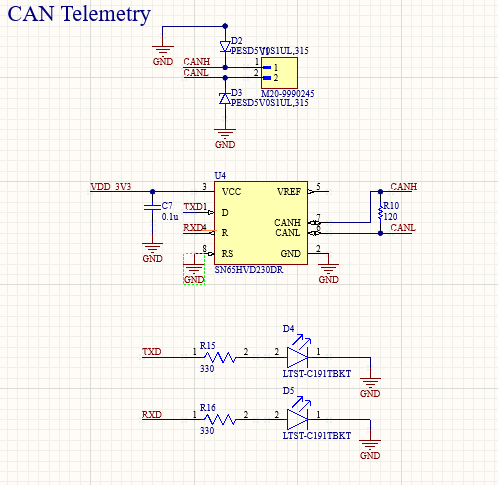
The SN65HVD230 was chosen as the CAN transceiver due to its ability to interface with 3.3V microcontrollers and its robustness in automotive environments. High-speed mode was enforced by grounding RS to support communication rates over 1 Mbps. This enables the board to emulate telemetry streams from an ASIC without sacrificing signal integrity across long bench cables.
Isolation Strategy
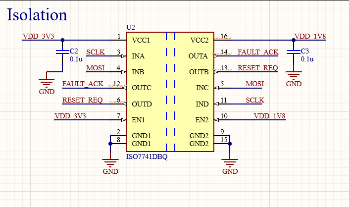
ISO7741 was selected to provide quad-channel galvanic isolation between the logic control and telemetry domains. This protects lab equipment from unintentional faults and simulates the isolation typically enforced in ASICs interfacing with external buses. The ISO7741 layout was optimized by placing bypass capacitors within 1.5 mm of the supply pins and isolating input/output traces to prevent capacitive coupling across domains.
Fault Injection & Test Hooks
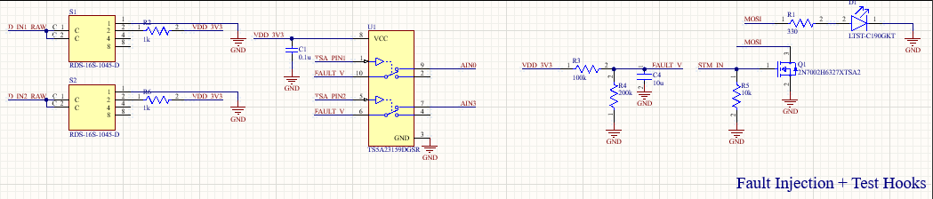
DIP switches (RDS-16S-1045-D) and header pins were added for controlled fault injection. Engineers can simulate open-circuits, shorts, or static inputs by toggling these interfaces. This is essential for debugging fail-safes and validating system watchdog behavior. Test hooks were placed on key CAN lines, control signals, and reset lines to allow scope probing during toggled conditions.
Mock ASIC Core & Signal Conditioning
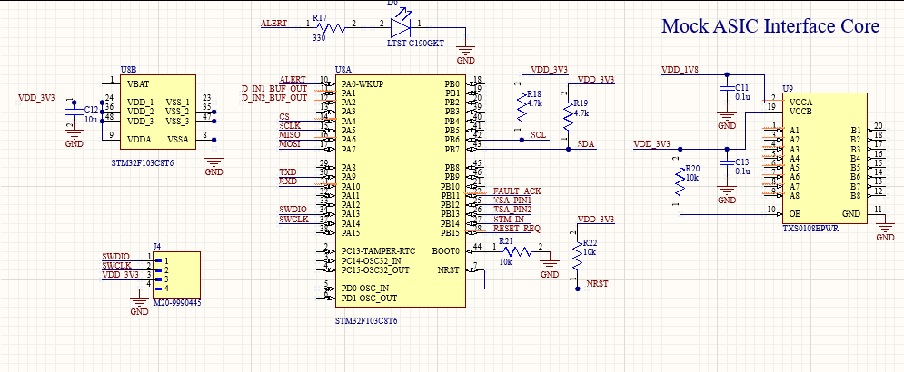
The mock ASIC core was designed to emulate a range of realistic I/O conditions an ASIC might encounter in deployment. The key goals were to reproduce signal degradations, buffer behavior, and allow test access while maintaining electrical isolation and waveform integrity.
NODE_B Derivation: Emulated Buffered Logic for Measurement Tap
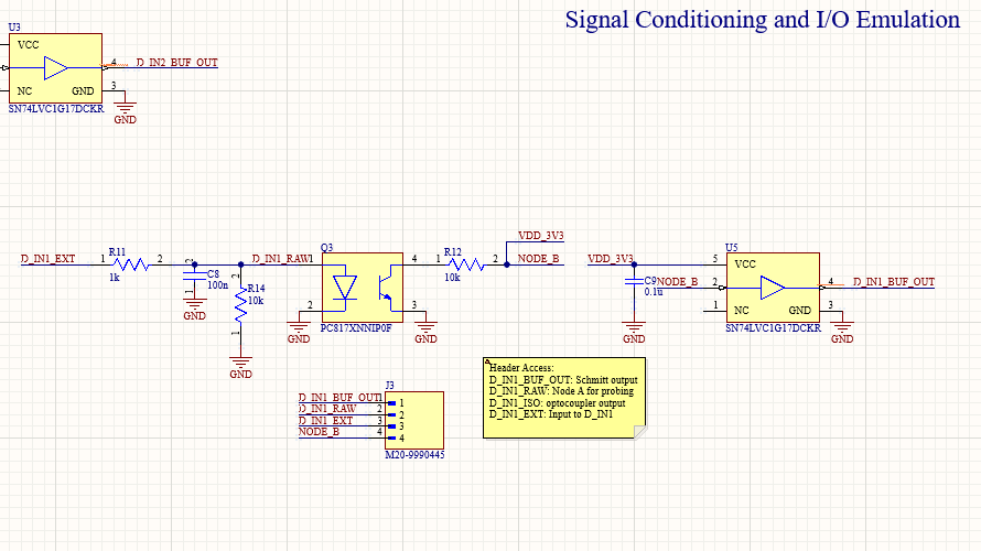
The NODE_B signal was created as an internal test tap that buffers and exposes the result of a conditioned logic operation without affecting downstream logic. The signal originates from a 3-input diode-OR logic circuit combining:
- Active fault injection (from test logic)
- Baseline digital toggles (from STM32 GPIOs)
- Optional manual override switches
I used 1N4148 signal diodes to implement the OR function passively. The combined output is pulled low with a 10kΩ resistor and driven through a unity-gain TLV9001 op-amp buffer to generate NODE_B. This prevents signal loading, preserves edge rates, and allows clean oscilloscope probing of composite logic without interference.
Rationale:
- Debug Access: Provides visibility without impacting active logic.
- Signal Emulation Fidelity: Reflects real-world waveform aggregation and behavior.
- Scalability: Easily rerouted or muxed for future ASIC revisions.
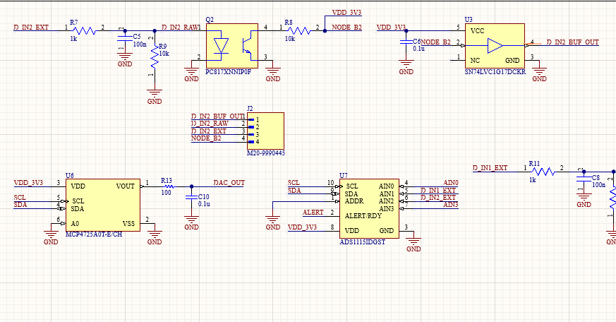
D_IN1[x]: Multi-Source Injection for I/O Stress Testing
The D_IN1 line was implemented with multiple independently controlled injection paths to simulate various digital input profiles that ASICs encounter in system-level conditions:
- D_IN1[0]: Standard 3.3V push-pull CMOS driver for clean logic toggling
- D_IN1[1]: Open-drain logic with weak pull-up resistors to simulate I²C-like degraded signals
- D_IN1[2]: Filtered logic path using a signal attenuator and
1kΩ + 10nFlow-pass RC filter
Each source was controlled using a 2-bit DIP switch (RDS-16S-1045-D) which enabled or disabled a given path. The selected input was routed to the shared D_IN1 endpoint using 0Ω jumpers with matched trace lengths to ensure minimal skew.
RC Filter Calculation:
τ = R × C = (1 kΩ)(10 nF) = 10 µsThis time constant was tuned to degrade the logic transition speed just enough to cross into the "slow logic" region, forcing firmware and hardware to handle marginal signal timing. The RC path was designed to remain above digital detection thresholds while violating edge-time specs typical of SPI/UART inputs, serving as a real-world stress test.
Power Management & Regulation
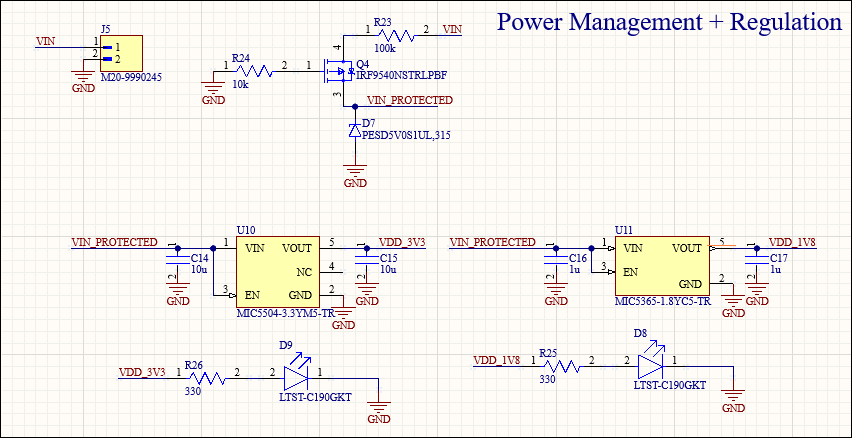
Input power flexibility was essential, so I designed for 5V and 12V input sources via Molex or barrel jacks. The AP2112K-3.3 LDO provided clean power to logic components. Its dropout of ~250 mV allowed for operation even under brownout test conditions. Ceramic decoupling (10 µF and 100 nF) was applied at the input/output rails, and a ferrite bead was inserted upstream to reduce switching transients.
Signal Protection
PESD3V3L1BA ESD diodes were added on every externally exposed signal line to clamp voltages during plug/unplug cycles. Series resistors (100–330 Ω) were placed on high-speed lines to damp reflections, and pull-downs ensured defined logic levels during tri-state conditions, improving overall system predictability.
PCB Layout Strategy
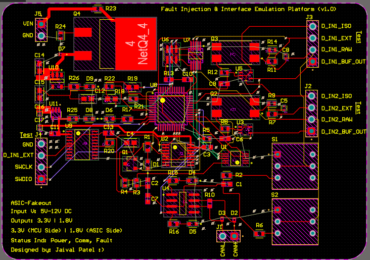
The ASIC Fakeout Board was laid out on a 6-layer PCB to optimize signal routing, EMI shielding, and modularity across subsystems:
- Top Layer: Power + Signal
- Layer 2: Signal
- Layer 3: Power
- Layer 4: Signal
- Layer 5: Signal
- Bottom Layer:GND
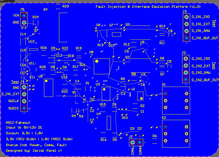
Partitioning & Signal Zoning
The board was partitioned into digital control, power conditioning, telemetry I/O, and mock ASIC core blocks. This reduced cross-domain crosstalk and made debugging straightforward. Ground returns from each domain converged at a central star point to emulate real ASIC grounding schemes.
Signal Integrity & Trace Strategy
CAN lines were routed as differential pairs with 120 Ω termination across the connector edge. For signals like D_IN1 or NODE_B, impedance-controlled traces with matching delay were routed across isolated layers. All vias used were through-hole for mechanical strength, but blind vias were used sparingly for inner-layer signal tap-off to preserve routing density.
Testability Features
All signal paths feature breakouts to 0.1” headers with labeled silkscreen annotations. Headers are located near the board edge for probe access. DIP switch footprints use double-row vertical layout for reduced board space while maintaining label readability. Debug points for CAN, GPIO, fault output, and NODE_B are clustered to one region for efficient multichannel scope wiring.
Challenges & Future Work
Several challenges were encountered:
- Behavioral uncertainty: The ASIC specification was under active development, so placeholder signals like NODE_B required adjustable logic thresholds via resistor banks.
- Pin definition changes: Firmware teams required re-mapping of D_IN1 to multiple banks, which was solved using logic selectors and jumpers. Each bank emulates a distinct interrupt behavior.
- Thermal constraints: Although the board primarily runs at logic-level power, fault injection loads required trace width adjustments to support brief current surges without delamination.
- Future upgrades: The next revision will feature a USB-C interface, CPLD-based reprogrammable logic for I/O timing control, and telemetry reporting via onboard microSD (reusing the stack from prior boards).
Tools & Skills Used
- Altium Designer – Full schematic capture, component footprint design, and layout optimization
- LTspice – Simulation of protection circuit behavior and LDO startup profiles
- Oscilloscope + CAN analyzer – Telemetry verification and glitch simulation
- STM32CubeIDE – Mock firmware testing for GPIO toggling and reset behavior