SmartInterfaceCore
Overview
SmartInterfaceCore is a 6-layer embedded interface bridge designed to isolate CAN bus communication, support fault detection and event logging, and offer modular ADC-based sensor interfacing for real-time diagnostics. It uses an STM32F103C8T6 as the central controller and supports microSD logging, RTC timestamps, and power failover.
The project was driven by the need to build a flexible, modular diagnostic interface that could integrate with both industrial CAN-based sensors and analog subsystems while offering protection from electrical noise, fault events, and poor power quality.
Key Features
SmartInterfaceCore was developed as a rugged, modular signal bridge capable of interfacing digital and analog sensors, isolating CAN bus communications, and supporting fault detection and telemetry logging. The board was designed to meet the demands of embedded systems used in electric vehicles, industrial diagnostics, and robotic actuator platforms. This section outlines the major subsystems and their design justification.
CAN Bus Isolation (ISO1042)
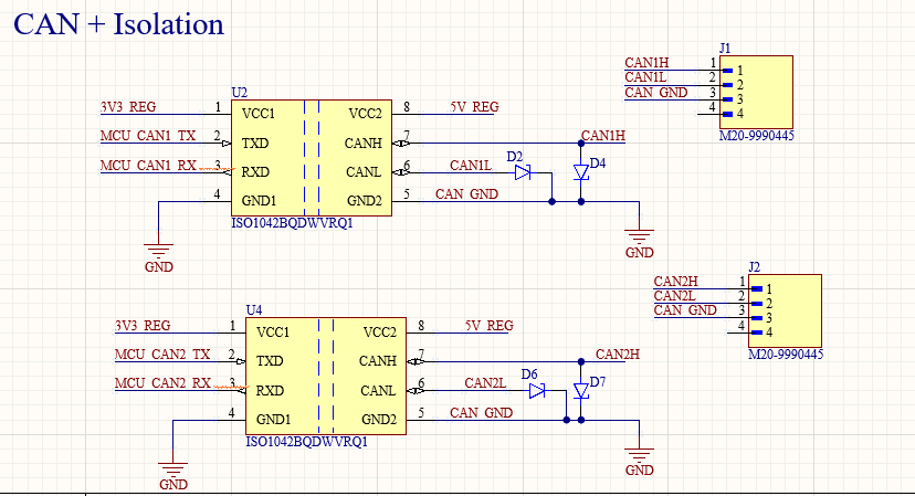
At the heart of the CAN interface is the Texas Instruments ISO1042, a high-speed isolated CAN transceiver compliant with ISO 11898-2. This part was chosen over standard transceivers like the SN65HVD230 to ensure galvanic isolation between high-voltage CAN domains and local digital logic, critical for applications where the SmartInterfaceCore is placed across different vehicle grounds or subjected to common-mode transients.
The ISO1042's reinforced isolation barrier allows 5000 Vrms withstand and ensures that noise from inductive loads on the CAN line (such as motors) doesn’t couple into microcontroller GPIOs. The differential CANH and CANL pins are routed as impedance-controlled pairs, terminated via 120Ω at the edge connector, with ESD TVS diodes placed within 5 mm of the connector.
Fault Detection & Protection Logic
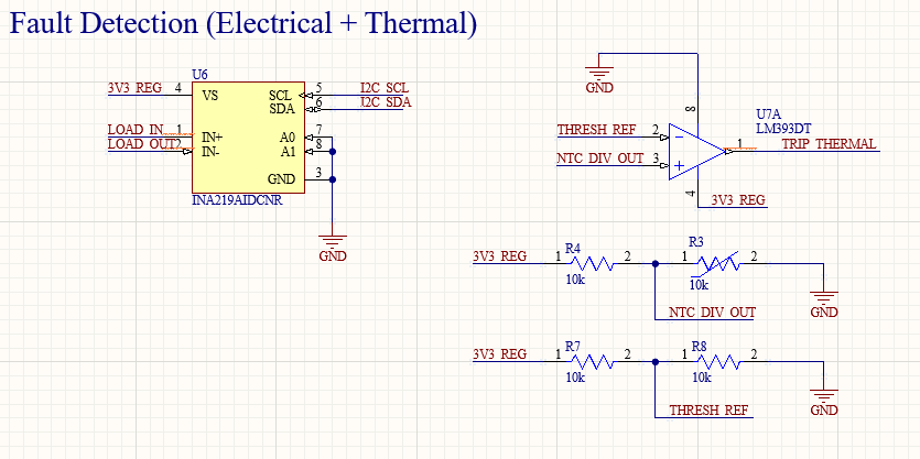
Fault detection was implemented through a combination of analog filtering, logic-level diagnostics, and programmable threshold detection. A key component in this system is the INA219 bidirectional current sensor, used to monitor the supply rail for abnormal current spikes that may indicate latch-up or peripheral failure. Additional open-drain pins on the STM32 allow for custom firmware-based GPIO latching logic when overcurrent or voltage deviation is detected.
Passive protections include a series fuse and reverse polarity protection diode, and capacitive filtering at each sensor pin header to suppress cable-induced spikes.
microSD and RTC Logging
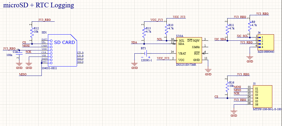
Logging capabilities are supported through an SPI-interfaced microSD connector and an I2C-linked DS3231 real-time clock (RTC). This system enables timestamped fault events, long-term sensor logging, and power-cycle event traceability.
The microSD connector follows the same tested pattern used in previous projects: SPI lines routed on a shielded internal layer with matched lengths, 10k pull-up on CS, and decoupled power via 10uF and 0.1uF near VDD. The DS3231 was selected for its temperature-compensated crystal oscillator, allowing it to maintain ±2 ppm accuracy over extended periods.
Power Management
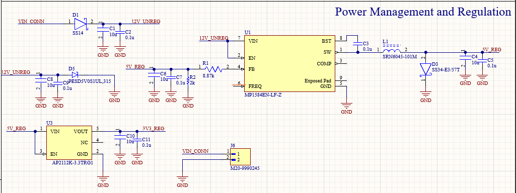
The power domain supports dual 5V and 3.3V logic zones regulated via an AP2112K-3.3 LDO, chosen for its low dropout, low quiescent current, and clean startup profile. This regulator provides stable 3.3V supply to the STM32, CAN transceiver, sensor ADC, and RTC.
Decoupling strategies include local bypass near each IC and ferrite beads between the 5V rail and sensitive analog domain. Reverse diode protection and a resettable polyfuse at the input rail prevent faults during incorrect supply or backfeed conditions.
Sensor Interface ADCs
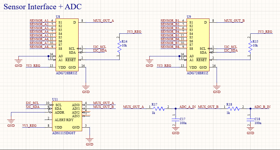
Sensor integration is handled by the ADS1115, a 16-bit, 4-channel I2C ADC with programmable gain. This device supports differential and single-ended measurements and was chosen for its low-noise front end and internal reference, suitable for measuring sensor voltages with microvolt precision.
GPIO-controlled enable logic allows sensor rails to be dynamically disconnected to reduce power draw or perform hot-swap behavior.
STM32F103C8T6 Controller
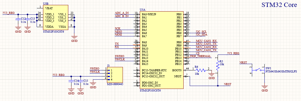
The STM32 was selected based on its:
- Built-in support for CAN, I2C, SPI, and UART
- Low power standby and watchdog timer support
- 12-bit ADC for fallback analog capture
- Community support and bootloader compatibility
The MCU is responsible for triggering log writes, handling sensor interrupts, forwarding CAN messages, and exposing debug telemetry via UART or USB. Its peripherals are distributed across multiple GPIO banks, with separate ground and power filtering near analog and digital blocks.
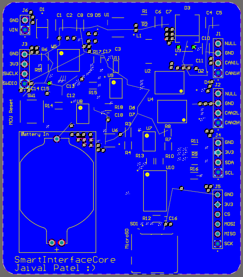
PCB Layout Strategy
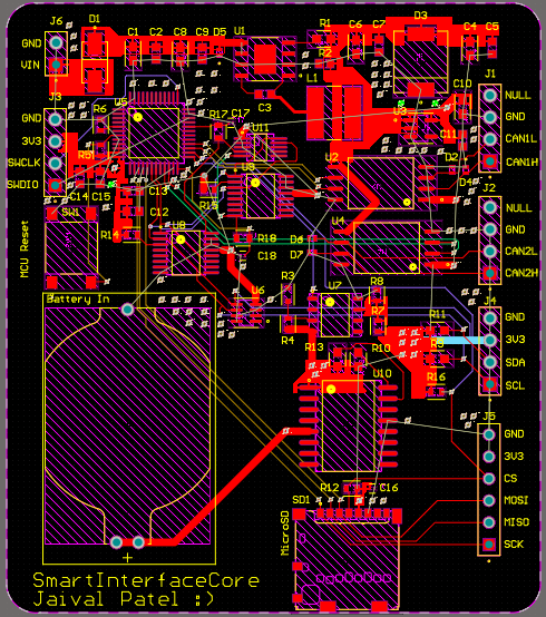
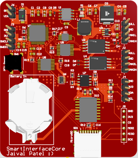
The SmartInterfaceCore uses a 6-layer stackup designed for robust signal isolation, noise resilience, and mechanical accessibility. Layout decisions centered on separating CAN, analog sensing, and digital logic across independent routing domains, with attention to decoupling, thermal relief, and ESD containment. All routing adhered to best practices for high-speed bus lines and low-noise analog front ends.
Layer Stackup
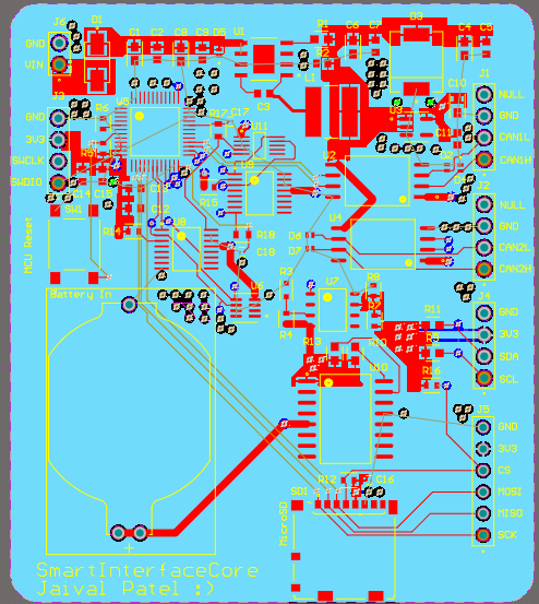
- Top Layer: Signal + components (STM32, CAN, ADC)
- Layer 2: Signal routing (sensor headers, UART, debug)
- Layer 3: Power plane (5V and 3.3V islands)
- Layer 4: Signal2 (CS lines, SPI, RTC)
- Layer 5: Signal3 (CAN_H/L, select logic)
- Bottom Layer: Continuous GND plane
CAN Domain Routing
The ISO1042 CAN transceiver was placed adjacent to the edge-mounted terminal block. CAN_H and CAN_L were routed as tightly coupled differential pairs with 120Ω termination placed close to the connector. The differential pair passed over a stitched GND return plane to maintain signal integrity, and ESD diodes were placed <5mm from the bus pins to suppress hot-plug transients.
STM32 Core Zone
The STM32F103C8T6 was placed centrally with short trace access to all peripherals:
- SPI routing to the microSD on Layer 4
- I2C routing to the DS3231 on Layer 2
- CAN TX/RX to the transceiver via Layer 5
- UART breakout and SWD headers on Top Layer
Power Distribution
Layer 3 includes dual 5V and 3.3V planes with ferrite bead filtering at rail entry points. The 3.3V domain feeds sensitive analog circuits, the STM32, RTC, ADC, and CAN driver. Copper pours connect power pins to these planes through short, wide traces with via stitching to minimize resistance and inductance.
Sensor ADC Layout (ADS1115)
The ADS1115 ADC was placed near the sensor headers on the board's left edge. Sensor traces were routed over GND with 20 mil spacing and input protection caps to suppress transients. I2C lines to the STM32 passed through a low-impedance return loop and were terminated with 10k pull-ups near the host controller.
microSD and RTC Pads
The SPI bus was routed underneath the STM32 to the microSD footprint using short, length-matched traces. Series resistors on CLK and MOSI prevent signal overshoot. The RTC pads were laid out for optional vertical mounting and maintain 4mm clearance from USB shielding zones to minimize coupling.
GND Stitching & Shielding
GND vias were stitched uniformly across all six layers, with increased density near high-speed or analog switching zones. The CAN domain has its own pour to isolate return noise, and every perimeter pad is connected to the ground flood to aid in ESD shunting.
Headers and Debug Access
All external-facing headers are labeled and aligned along the edge of the board for logic analyzer probe access. The UART and SWD headers are orthogonally spaced to prevent tool collision during debugging.
MATLAB Simulation Results
Simulation Objective
This simulation models the analog sensor input and fault detection threshold used in the SmartInterfaceCore ADC interface. It evaluates how noise, signal drift, and transient conditions influence detection reliability and informs the design of filtering and thresholding strategies.
Simulation Code in MATLAB
t = 0:0.01:10;
adc_input = 1.65 + 0.3*sin(2*pi*1*t) + 0.05*randn(1,length(t));
threshold = 2.8;
fault_detected = adc_input > threshold;
plot(t, adc_input); hold on;
yline(threshold, 'r--', 'Fault Threshold');
xlabel('Time (s)'); ylabel('ADC Voltage (V)');
legend('Sensor Signal','Trip Level');
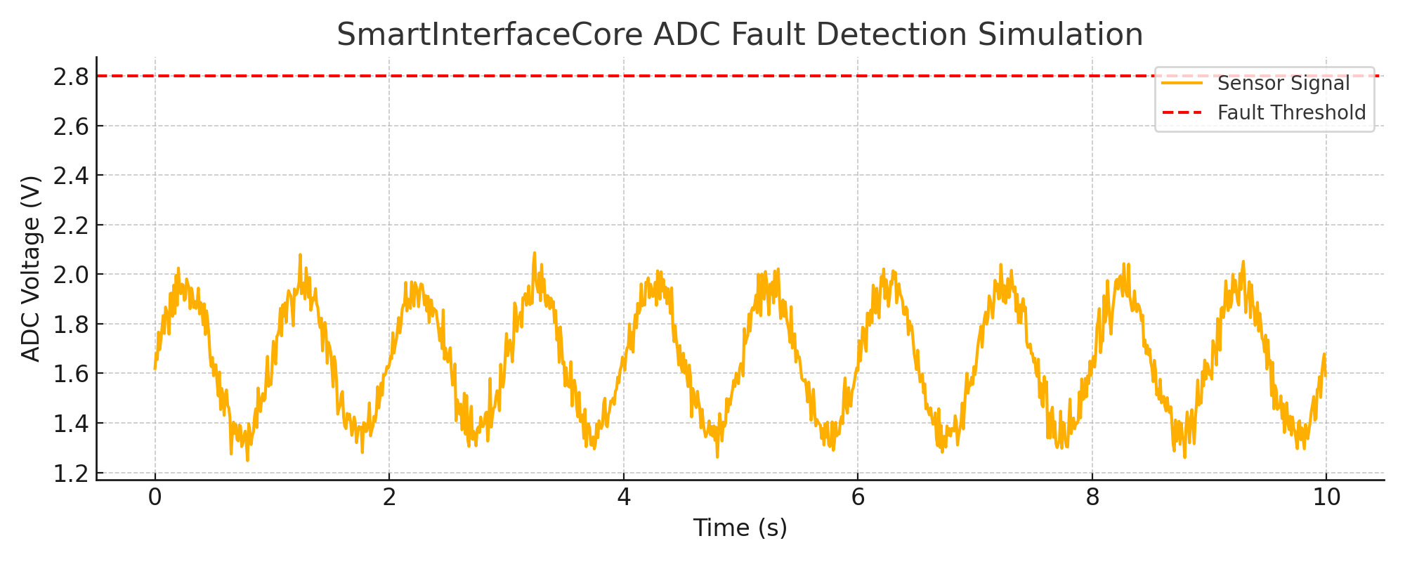
The simulated signal demonstrates typical behavior of a noisy analog sensor operating near a defined fault threshold. In this case, the threshold was chosen based on the operating range of a 0–3.3V ADC, with fault events defined as voltages exceeding 2.8V.
Transient spikes cross the threshold multiple times, highlighting the risk of false positives in high-noise environments. These results inform firmware design by emphasizing the need for either:
- Moving average filtering (digital)
- Analog RC filtering
- Multi-sample threshold confirmation logic
This analysis confirms the responsiveness of the SmartInterfaceCore ADC subsystem under analog variability and suggests fault filtering tradeoffs between speed and precision. It also validates the ADS1115’s high-resolution front end, which is capable of capturing these dynamics without clipping. Firmware-level debounce, fault latching, and averaging will be implemented to enhance reliability in final deployments.
Challenges & Debugging
- CAN transceiver ESD fault fixed with updated TVS diode package
- microSD CRC errors resolved via SPI re-timing and decoupling capacitor tuning
- INA219 current spikes filtered with ferrite bead + ceramic cap network
- RTC communication stabilized using 10k pull-ups and edge-cleaned SDA/SCL routing
Tools & Skills Used
- Altium – 6-layer PCB design and layout
- STM32CubeIDE – SPI, I2C, CAN, and ADC firmware integration
- MATLAB – Fault simulation and signal filtering evaluation
- CANalyzer + oscilloscope – Bus analysis, sensor timing validation
Future Work
- Expand to dual CAN-FD channels
- Add overvoltage trip with external comparators
- Support MODBUS via RS485 for industrial bridging
- Optimize data logger with FAT32 filesystem streaming